IC Package Illustrations, From 2D To 3D
In five words or less can you describe what a semiconductor is? Some might say a computer chip, others may say they are “space magic,” but I would venture that certain people have never heard the word before and would simply say “I have no idea.” I was certainly a part of the latter crowd before I began my internship with Amkor Technology where I was brought on board as a 3D illustrator to create realistic package illustrations. Now, after 3 years in this role, I can confidently say that semiconductors are the “devices that connect our world.”
It is no secret that many of the semiconductor illustrations across the internet paint a decent enough picture of the form and function of a package and how the substrate, die(s), or components stack up. However, a lot of times these illustrations are drawn up in PowerPoint or Word (figure 1), where they are crude, granular, or not to scale due to the limited feature set of these programs. Not only that, but when images get cropped or re-shared constantly, the images tend to get compressed or reduced in quality and the original message the artist or engineer wanted to convey gets lost in the pixels. When it comes down to communicating the concepts of certain packages to our customers and colleagues, accuracy, realism, and quality become non-negotiables.
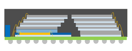
Fig. 1: M.2 Module PowerPoint cross-section
Throughout my internship, I utilized Dassault Systèmes’ SOLIDWORKS computer-aided design (CAD) software to draw substrates, dielectrics, solder masks, vias, dies, wirebonds, and anything else you can think of that is within a semiconductor package. What started out as flat, block-like images now have depth and scale that can be interpreted by a customer or engineer. What really elevates the package illustrations comes from the material database found natively within the program. Here I can make solder masks appear green and polymer-like, wirebonds as gold, silver, or even epoxy, and underfill as viscous. The opportunities are endless and the ability to export these files as realistic renders sets them apart from their counterparts.
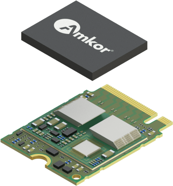
Fig. 2: M.2 Module SOLIDWORKS 3D isometric rendering
Redrawing package illustrations has become an important part of my workflow and the more I learn about semiconductor packages, the more accurate my illustrations can become, and thus the more intellectual information Amkor can have at its disposal. Rendering cross sections, creating 3D isometric packages (figure 2) that show internals, or even generating new package concepts with the guidance of engineers has become a staple of the brand that I have been able to support here at Amkor. In this role, I am thankful for the opportunity to help our engineers and customers to conceptualize semiconductor packages a little bit better.
About the Author
Tyler DeHaan joined Amkor in 2020 and currently works in the R&D Design Center as a design engineer creating complex and in-depth 2D & 3D IC package illustrations. He previously served as a 3D Illustration intern in Amkor’s Marketing Communications department. DeHaan holds a bachelor’s degree in mechanical engineering from Arizona State University.
Related Posts
Amkor Technology Launches Semiconductor Educator Bootcamp to Strengthen Future Workforce Pipeline
Amkor Showcases Next-Gen Packaging and U.S. Expansion at ECTC 2026