
Implement any packaging scheme with Wafer Level Packaging
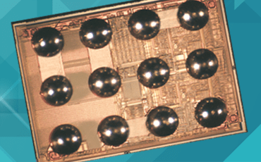
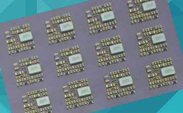
Amkor offers a broad array of Wafer Level Packaging (WLP) capabilities and processes for packaging schemes from fan-out to chip scale to 3D to System-in-Package (SiP). Our advanced manufacturing operations in Korea, China, Taiwan, and Portugal are adjacent to major foundries, enabling the integration of factory logistics and reducing time-to-market.
The WLP family is applicable for a wide range of semiconductor device types while leveraging the smallest form factor and high performance from high-end RF WLAN combo chips, to FPGAs, power management, Flash/EEPROM, integrated passive networks and standard analog.
Looking for technical information?

Data Sheets

Brochures

White Papers
