
Next generation bump technology for greater density, reliability and performance
Copper pillar bump is widely used for many types of flip chip interconnect which offers advantages in many designs while meeting current and future ROHS requirements. It is an excellent interconnect choice for applications such as transceivers, embedded processors, application processors, power management, baseband, ASICs and SOCs where some combination of fine pitch, ROHS/Green compliance, low cost and electromigration performance are required.
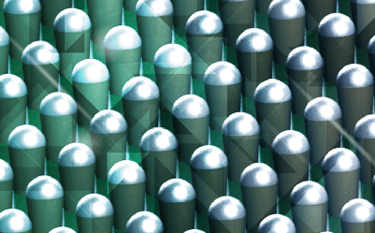
Benefits of Copper Pillar
- Fine pitch capable down to 30 μm in-line and 30/60 μm staggered
- Superior electromigration performance for high-current carrying capacity applications
- Electrical test at wafer level prior to copper pillar bump
- Compatible with bond pad opening/pitch and pad metallization of die designed for wirebond which enables quick time-to-market for conversion to flip chip
- Cost reduction achievable in many designs by reducing substrate layer counts
- Lower cost fine pitch flip chip (FPFC) interconnect versus Au stud bump for high bump density designs
- Various Cu pillar structures available from Cu bar type, standard Cu pillar, fine pitch Cu pillar and micro-bumps. Also, available in different stack-ups from Cu+Ni+Pb-free, Cu+Ni+Cu+Pb-free depending upon application requirements
- Available with and without repassivation
- Qualified for advanced silicon node Low-k devices
- Small fillet requirement for underfill enables more aggressive die‑to‑package design rule/smaller package footprint
- Extreme fine pitch on silicon package down to 30 μm for TSV and CoC
Questions?
Contact an Amkor expert by clicking the request info button below.