
Packages for improved warpage control and integrity
Portable electronic products such as mobile phones, digital cameras, gaming and other mobile applications can benefit from the combination of stacked package and small footprint offered by the package-on-package (PoP) family.
Amkor is committed to maintaining strong development and production capabilities to ensure we are at the forefront in meeting next generation PoP requirements such as, higher density stacked interfaces in combination with PoP mounted area and height reductions.
Package Stackable Very Thin Fine Pitch BGA (PSvfBGA), launched in 2004, supports single and stacked die using wire bond or hybrid (flip chip plus wirebond) stacks to improve flip chip warpage control, package integrity through test and SMT handling.
Package Stackable Flip Chip CSP (PSfcCSP) enables the use of an exposed die bottom package, integrates the package stacking design features of PSvfBGA in an fcCSP assembly flow, in our PSfcCSP package. PSfcCSP has a thin exposed flip chip die enabling fine pitch stacked interfaces at 0.5 mm pitch, which is a challenge in a center molded PSvfBGA structure.
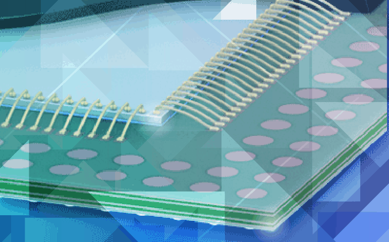
Through Mold Via Package-on-Package (TMV® PoP) is our next generation PoP solution with interconnect vias through the mold cap. TMV provides a stable bottom package enabling the use of thinner substrates with a larger die to package ratio. TMV-enabled PoP can support single, stacked die or flip chip designs. This technology is an ideal solution for 0.4 mm pitch low power DDR2 memory interface requirements and enables the stacked interface to scale with solder ball pitch densities to 0.3 mm pitch or below.
Questions?
Contact an Amkor expert by clicking the request info button below.