
Meeting industry demands for turnkey WLCSP products
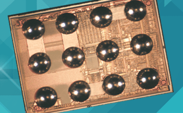
Amkor Technology offers Wafer Level Chip Scale Packaging (WLCSP) providing a solder interconnection directly between a device and the motherboard of the end product. WLCSP includes wafer bumping (with or without pad layer redistribution or RDL), wafer level final test (probe), device singulation and packing in tape & reel to support a full turnkey solution.
Amkor’s robust Under Bump Metallurgy (UBM) over PBO or PI dielectric layers on the die active surface provides a reliable interconnect solution able to survive harsh board level conditions meeting the demands of the growing global consumer market place for portable electronics.
The WLCSP package family is applicable for a wide range of semiconductor device types from high end RF WLAN combo chips, to FPGAs, power management, Flash/EEPROM, integrated passive networks, standard analog and some automotive applications. WLCSP offers the lowest total cost of ownership enabling higher semiconductor content while leveraging the smallest form factor and one of the highest performing, most reliable, semiconductor package platforms on the market today.
Amkor offers three WLCSP options
- CSPnl Bump on Repassivation (BoR) option provides a reliable, cost-effective, true chip-size package on devices not requiring redistribution. The BoR option utilizes a repassivation polymer layer with excellent electrical/mechanical properties. A UBM is added, and solder bumps are placed directly over die I/O pads. CSPnl is designed to utilize industry-standard surface mount assembly and reflow techniques.
- CSPnl Bump on Redistribution (RDL) option adds a plated copper Redistribution Layer (RDL) to route I/O pads to JEDEC/EIAJ standard pitches, avoiding the need to redesign legacy parts for CSP applications. A nickel-based or thick copper UBM offerings, along with polyimide or PBO dielectrics, provide best in class board level reliability performance. CSPnl with RDL utilizes industry-standard surface mount assembly and reflow techniques and does not require underfill on qualified device size and I/O layouts.
- CSPn3 option utilizes one layer of copper for both redistribution and UBM. This simplified process flow reduces cost and cycle time by over 20%. CSPn3 has been in production since 2009 and has a run rate of over 4 billion units since its introduction.
Questions?
Contact an Amkor expert by clicking the request info button below.