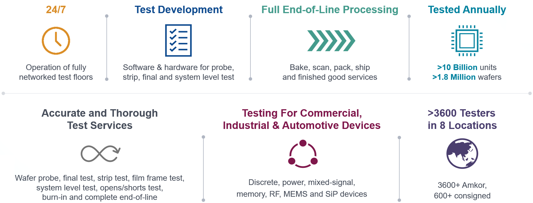
Innovative test solutions for diverse semiconductor system applications
凭借数十年来支持一流和新兴行业领袖所积累的知识,Amkor 了解测试解决方案测试的先进技术、质量、性能和成本问题。通过在前期参与到每个客户的产品周期当中,Amkor 帮助确定测试策略与选择智能设备,并提供差异化的测试解决方案。
Amkor offers comprehensive test services, including and not limited to, wafer level and package assembly. Amkor is the leading RF test services supplier and is engaged in ongoing joint efforts with test equipment suppliers and customers to enable 5G product production testing. As the top OSAT supplier for high-performance compute (HPC), artificial intelligence (AI) processors & automotive testing, we have an extensive array of test capabilities and significant experience in device testing. The performance envelope for Burn In and System Level Test have recently expanded, to account for higher power and lower cost.
测试设备
Amkor 拥有大量的设备,而且继续投资是自己具备相应的能力,以测试最新器件
Application
- High-Performance Compute, AI, Power, Memory, Analog, RF, MEMs, Sensor, SiP
测试仪
- Clock: PEC clock rate, differential clocks, low Jitter, levels
- I/O: At-speed functional test. Low- & high-speed data I/O differential buses. Peripheral Event Controller (PEC) channel count, levels, timing – low EPA, patterns, test & measurements
- Power Delivery: Device power supply – channel count, levels, ganging, source and measure, high accuracy
- RF & Analog I/O: RF source & measure FE with optimal Rx/Tx port count to allow max parallelism for max UPH; ADC/DAC – resolution, accuracy, dynamic range to enable testing the latest technologies
- 针对最大 UPH 的最优化平行度
负载板
- PCB Material, PCB width, Trace impedance
- Per pin current capability, Pin-to-pin crosstalk
- 对工具的 RFID 监控
- 温度容限
Test Socket
- Per pin current capability, Pin count per DUT, Pin field planarity
- 引脚之间串音/隔离/屏蔽
- 温度容限
分选机
- 自动温度控制/热浸
- DUT 旋转
- Footprint, Loading force, Loader speed
- Package handling, Position XY accuracy
Application
- Die Sales – Low-power apps
- Chiplets – 2.5D, 3D – μBumps, Hybrid bonding
- 硅光子
测试装置
- 高速逻辑、混合信号、模拟、大功率和 RF
- 探针引脚数据速率、电流密度和经济的平行度
探针
- Wafer Size – 8” and 12” with 7, 5, 3, 2 nm process technologies
- Chuck planarity, Loading force, Position XY accuracy, Rotational angle
- Temperature Range
- Reconstituted wafers
探针卡
- 全部对接类型,如缆线、探针塔、直接对接
- In-line LASER cleaning; Overdrive
- Probe card technologies: Cantilever, vertical, pogo, membrane, MEMS & dual-level Chip-on-Wafer (CoW)
- 接触次数
- 每 DUT 的引脚数量;引脚之间串音;每引脚电流能力
- Pin field planarity; Alignment accuracy
Temperature tolerance
Application
- Logic, Memory, Automotive
- Sub 30W, Up to 200W, Up to 1000W
- Wafer Level & Package Level
- Massively parallel test insertion
老化测试仪
- 高区/测试箱数量
- 最大时钟频率
- 最大 I/O 通道数量
- 最大插槽数量
- 产品认证和 100% 老化测试支持
- 功率区段宽
老化板
- DUT 功率输出:支持所有电源应用 IC
- 支持 I/O 和时钟频率
- 引脚之间串音:针对大多数(即使不是全部)应用控制在最低程度
- 插座配置和功能
- 成本敏感型插座,引脚减数和引脚偏置
- 高温容限
老化分选机
- 老化板 (BIB) 装卸机
老化装卸机 (BLU)
- 支持全部主流封装类型
- 高效输入和输出
- 手动元件和 BIB 装卸:不建议用于大批量和 100% 老化,或者对周期时间效率有要求的测试
Application
- High-Performance Compute, Automotive, SiP
- Massively parallel test insertion
系统级测试仪
- Clock Rate: High
- I/O: Max slot count, max I/O channel count
- Power Delivery: Range ultra-low, low, medium, high, rail count
- 每小时最大单位数
系统级测试板
- DUT power delivery – all power application ICs
- supported
- 支持 I/O 和时钟频率
- 引脚之间串音 – 针对大多数(即使不是全部)应用控制在最低程度
- 插座配置和功能
- 成本敏感型插座,引脚减数和引脚偏置
- 高温容限
系统级分选机
- 高测试样式区数量
- 产品认证和 100% 支持
- 系统级装卸机
- 支持全部主流封装类型
- High-efficiency I/O
- 温度控制器 – 低温浸泡开销分时
完全可定制的后端制程
- 后期打标可选,是否烘烤取决于湿度敏感级别 (MSL)
- 对于小型转塔式分选机封装,将按顺序执行最终测试、扫描和卷带包装。
适用于先进封装的先进解决方案
- 层叠封装 (PoP)
- Through Silicon Vias (TSV)
- Flip Chip CSP (fcCSP)
- Flip Chip BGA (FCBGA)

测试地点
Our sites are strategically located near leading foundries, and major customer sites and co-located to support probe and test with assembly
Amkor Technology China (ATC) is located in the Pilot Free Trade Zone, which is only about 30 kilometers from two primary airports in Shanghai. The Free Trade Zone’s convenient logistics and business-friendly policies allow Amkor customers to deliver goods around the globe through value-added taxes or tax exemptions. ATC has 170,000 square meters of manufacturing space.
产品
- 晶圆探针测试
- 膜片架测试
- 封装测试
- Burn-in test
- 系统级测试
- 测试开发
封装
- CSP
- FCBGA
- 倒装芯片
- MLF®/QFN
- PBGA
- WLCSP
市场
- 汽车
- 通信
- 消费品
- 工业
Amkor Technology Japan (ATJ) is located in Japan with seven factories and a head office. The head office is in Tokyo, which is only around 16 kilometers from HND airport and 5 kilometers from Tokyo station. The factories are located all over Japan and the diversified manufacturing footprint is a key differentiator/competitive advantage that allows customers options to de-risk supply chains. ATJ has test experience with various semiconductor devices, e.g. Mix analog, Power discrete and module, System LSI and CIS and has 170,000 square meters of manufacturing space.
产品
- 晶圆探针测试
- 封装测试
- 测试开发
封装
- 倒装芯片
- PBGA
- QFN
市场
- 汽车
- 通信
- 存储器
Amkor Technology Korea (ATK) operations encompass more than 11M ft2 of floor space with production facilities, product development centers, and sales and support offices strategically located in key electronics manufacturing regions. Our customers benefit from our extensive global footprint, enabling us to easily handle large orders and offer quick turnaround times. Our diverse portfolio includes stacked die, wafer level, MEMS, flip chip, Through Silicon Via (TSV) and 2.5/3D packaging, allowing us to be a single source for many customers. The ATK5 & ATK3 are about 34 kilometers away from Incheon airport. ATK4 is in the south of SKorea 335 kilometers from the Incheon airport.
产品
- 晶圆探针测试
- 封装测试
- 膜片架测试
- 系统级测试
- 测试开发
- 凸块
封装
- FCBGA
- fcCSP
- MLF®
- TQFP
- TMV®
- TSV – 2.5D, 3D
- WLCSP
市场
- High-Performance Compute (HPC)
- Artificial Intelligence (AI)
- 汽车
- 通信
- 消费品
Amkor Technology Malaysia (ATM) is located in Malaysia’s Free Industrial Zone, about 50 kilometers from Kuala Lumpur city center and Kuala Lumpur International Airport. The Free Trade Zone’s convenient logistics and business-friendly policies allow Amkor customers to deliver goods around the globe through value-added taxes or tax exemptions. ATM has 32,000 square meters of manufacturing space and 108,800 square meters of land.
产品
- 封装测试
封装
- SO8-FL
- SONXXX-FL
- TO-220FP
- TQFP
- TSON-FL
市场
- 离散
- 功率
Amkor Technology Philippines (ATP) provides a full range of assembly and test services. ATP has two factories located in Muntinlupa City (P1) and Binan City, Laguna (P3/P4) to serve our global clientele. ATP P1, Muntinlupa City – has a manufacturing space of 32,000 sqm that is dedicated to producing legacy lead frame products.
ATP P3/P4, Binan City, Laguna, with a size of 32,800 sqm, is leading the way in advanced packaging technologies. P3 Assembly is recognized for its advanced packages and serves as a manufacturing and development center for MEMS and sensors. Amkor’s testing facility in P4 has been offering wafer probe and final testing services for the past 30 years, managing a wide range of applications including power and microcontrollers to MEMS.
With ATP registered with the Philippines Economic Zone Authority (PEZA), Amkor customers can enjoy significant benefits. The benefits consist of shipping products worldwide with incentives, VAT zero rating, and preferential tax rates, which guarantee a cost-efficient and efficient supply chain.
ATP has earned a reputation for its reliable packaging technology innovations and testing facilities. Our operational base encompasses both production and product development, which enables us to meet the changing demands of the semiconductor industry.
产品
- 晶圆探针测试
- 封装测试
- 膜片架测试
- 系统级测试
- 测试开发
- MEMS Test
- 老化
封装
- MLF®
- 引脚框架
- QFP
市场
- 汽车
- 消费品
- 存储器
Amkor Technology Portugal (ATEP) is located near Porto, the second biggest city in Portugal and fifteen minutes away from the international airport and seaport with excellent direct connections inside Europe and to the rest of the World. Being the biggest Outsourced Semiconductor Assembly and Test facility in Europe, dedicated to Advanced Packaging, the location benefits from accumulated Semiconductor Assembly and Test experience in the region for more than five decades. ATEP currently has 20,000 square meters of clean room space and is expanding to 50,000 square meters.
产品
- 晶圆探针测试
- 测试开发
封装
- FCBGA
- WLCSP
- WLFO
市场
- 汽车
- 通信
- 存储器
ATT is situated in the HsinChu scientific area’s Taiwan Semiconductor Circle ecology, and it takes 30 minutes to reach the airport and wafer foundries. With Full-TurnKey solution services that include Bump/CP/WLCSP & Bump/CP/FCBGA/FT, Amkor Technology Taiwan (ATT) focuses on advanced packages (Bump, WLCSP and FCBGA). Additionally, ATT provides RD resources to help clients with complete solution design, including package, test program, and assembly development. ATT has 48,000 square meters of cleanroom manufacturing space.
产品
- 晶圆探针测试
- 封装测试
- 膜片架测试
- 凸块
封装
- Bumped wafer
- WLCSP
- fcCSP
- FCBGA
- SiP
市场
- 通信
- 消费品
- 网络
Amkor Technology Vietnam (ATV) is situated in Bac Ninh, and it takes 25 minutes to reach the airport. This site provides System-In-Package and Memory package and test services. Additionally, ATV provides RD resources to help clients with complete solution design, including package, test program, and assembly development. ATV has a large area of cleanroom manufacturing space.
产品
- 最终测试
- 系统级测试
- 测试开发
封装
- SIP – SoC, SoC
+ Memory PoP, double sided stacked - 存储器
- AiP, AoP
市场
- 通信
- 消费品
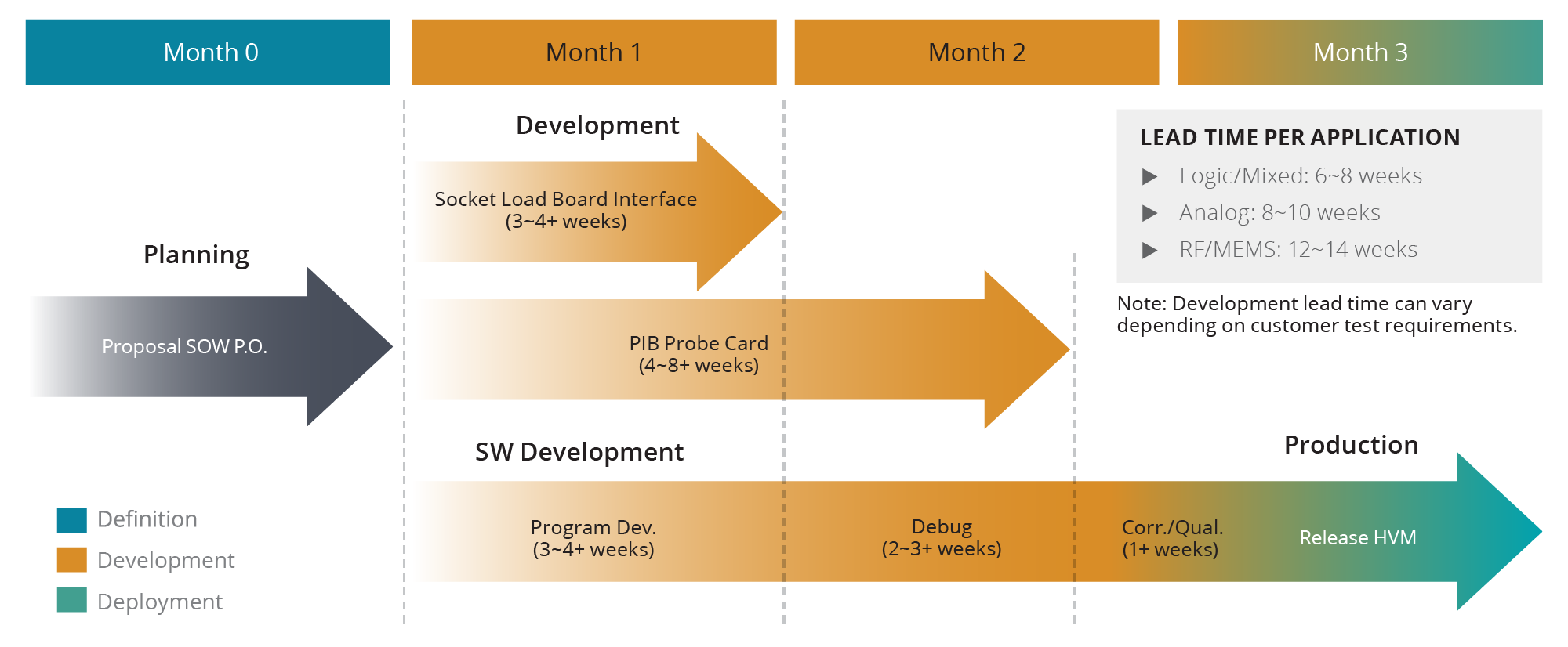
测试开发工程
小部分客户会自己开发完整的测试解决方案,然后交由 Amkor 执行。Amkor 有能力协同开发,或者独立开发完整的测试软件和硬件解决方案。在产品设计的前期与我们合作,收获更大程度的效益,或在产品周期的后期联系我们,通过转用更具有成本效益的测试装置和/或更高的平行度,以便于节省大量的成本。
典型的测试开发周期时间
不同市场的差异化测试
Amkor is the number one automotive OSAT, supporting worldwide supply chains. Products in this area include infotainment and safety (ADAS) requiring high levels of performance. This requires a comprehensive set of test during the production test workflow.
- Cold wafer probe, room & hot temperature final test
- 高质量,符合标准的制程与系统
- Inspections and multi-temperature test capabilities
- 晶圆探针温度从 -55°C 到 +200°C
- 最终测试温度从 -55°C 至 +175°C
- 老化
- 系统级测试 (SLT)
- 低温晶圆探针,并且进行室温和高温最后测试
- Post-assembly opens/shorts testing includes 2 and 4-wire resistance tests
The largest fraction of Amkor’s revenue is derived from the Communications market segment. This includes smartphones, tablets, handhelds and wearable devices. Our leading-edge test solutions keep pace with rapid changes in cellular and connectivity technology requirements. Amkor is well-positioned for 5G RF wireless products and their test requirements.
- RF 5G NR Conductive test for both FR1 and FR2 frequency ranges
- Asynchronous test for a multitude of RF connectivity standards
- ATE,具有 32 个端口和多站点、多通道 Tx 和 Rx 支持
- 通过简单的 SLT(包括 RF 呼叫测试)解决复杂的 SiP 问题
- 本地 RF 屏蔽效果≤ 60 dBm
- 多同测数 x8 RF 测试以降低成本
- RF 前端 (RFFE)、SiP 和 IoT
- RF 晶圆探针能力—WLCSP 的良裸晶片 (KGD) 和 SiP 的已测晶片 (KTD)
- 单通道和多通道聚束、相位阵列、AiP/AoP 支持
- SoC + 存储器 PoP—双面测试/堆叠 CSP—存储器和逻辑测试
Amkor is a leading provider of high-performance test solutions for the demanding networking and high-performance compute market. This market segment is driving the need for multiple chiplets that include artificial intelligence (AI) accelerators, central processing units (CPU), graphics processing units (GPU), field-programmable gate array (FPGA), input/output (I/O), serializer/deserializer (SERDES – PCIe, CXL), silicon (Si) photonics. Integral to these markets are advanced memory technologies like high bandwidth memory (HBM) and migrations from hard disk drives to solid-state drives (SSD), with NAND memories.
- Distributed test (wafer probe, in-situ test between key assembly steps and final test (SLT and ATE) for 2.5D & 3D). Probe solutions and wafer map management for chip-on-wafer (CoW)
- Active thermal control (ATC) for up to 300-watt & up to 1000W products across tri-temperature in SLT and ATE test
- Dynamic burn-in. Test during burn-in (TDBI)
- 膜片架和条状测试 (x308 EEPROM)
- 高速串行数字(如,PCIe Gen4、Gen5)测试,最高达到 16 Gbps 和 32 Gbps
- 硅光子集成电路
Amkor is a leader in power discrete devices & modules like Diodes, Flip chip MOSFETs, Intelligent power modules, Insulated-Gate Bipolar Transistors (IGBT), Multi-voltage FETs, Regulators and bipolar transistors for the automotive, power transmission and industrial segments. Amkor’s test services are closely integrated with the assembly flow for shorter cycle times and reduced costs. Key characteristics include:
- 大电流,高电压
- Kelvin 接触测试
- 低 Rds_on
- Si, SiC, Gan
Products for today’s Internet of Things (IoT) and Industrial Internet of Things (IIoT) require an MCU, RF transmitter/receiver, sensors and actuators. Sensor technologies include and are not limited to magnetometers, accelerometers, gyroscopes, proximity, RF switches, photo sensors, microphones, micro-speakers, humidity, pressure, and temperature. The test solution needs to cover the conversion of these physical real-world analog signals in a variety of range of operations into an electrical stimulus that is tested during the production workflow.
测试封装
运营
- 在 125°C 环境下的铜柱 (CuP) 凸块
- 高温/低温测试能力
- No Micro-Bump probe – Lack of demand
测试解决方案
- 全部 ATE 种类
- 探针卡与产品的功能要求相符
- 翘曲处理探针
当前产品
- 汽车雷达收发器/接收器、压力传感器和网络交换机
- RF 调谐器、基带、收发器、交换机、PMIC、GPU
- WLCSP, WLFO, CuP, leadframe bump, CoW, SiP, CoC, and 2.5D/3D TSV
运营
- O/S、KGD/介质层、TSV 测试
- 封装最终测试/SLT
测试解决方案
- C/P: Approaching 50 µm pitch, >35K needles, >100A, tri-temp
- F/T: Tri-temp, ATC >300W
- O/S:2/4 端 Kelvin
- SLT: 12 sites, ATC >300W
当前产品
- 逻辑 + 存储器 + 硅介质层、3D TSV HBM、HMC
- 移动 AP、CPU、GPU
- 网络、服务器
运营
- 老化
- 最终测试
- 系统级测试
测试解决方案
- 接触器波导设计
- Firmware-based PC test
- 多通道 RF 连接标准
- 适用于 RF 呼叫测试的 SLT 分选机
当前产品
- Flip chip Tx/Rx @ 24/53 GHz for mmWave
- 适用于 WiGig fcCSP (60 GHz) 的合格 BOM 量产
- RF 前端模块
- WLFO Qualified for 60GHz & 80GHz bands
运营
- Final Test and SLT test steps
测试解决方案
- Asynchronous test for a variety of RF connectivity standards
- 针对模块测试的接触器设计
- Firmware-based PC test
- Slot-based SLT handler for massively parallel test
当前产品
- 先进 SiP、PoP、DSBGA、堆叠晶片、封装内封装 (PiP)、空腔、面对面 (F2F) 及其他
- RF 前端模块
- 汽车/PMIC/MEMS/EMI 屏蔽/IPD
运营
- SOC + 存储器 PoP
- 双面测试/堆叠 CSP
- 存储器和逻辑测试
测试解决方案
- 通过逻辑或调制解调器晶片进行存储器接口测试
- 通过逻辑晶片进行 SLT 存储器测试和存储器保险丝熔断
- 顶部/底部插座
当前产品
- 小节距 TMV®/介质层 PoP
- 移动 AP & BB PoP
- 移动调制解调器和存储器堆叠 CSP
有问题?
点击下方的 “获取信息“ 按钮,
联系 Amkor 专业人士。