Thermal Simulation of DSMBGA & Coupled Thermal-Mechanical Simulation of Large Body HDFO
Electronic packaging has continued to become more complex with higher device count, higher power densities, and Heterogeneous Integration (HI) becoming more common. In the mobile space, systems that were once separate components on a printed circuit board (PCB) have now been relocated along with all their associated passive devices and interconnects into single System in Package (SiP) style subassemblies. High-power computing and data center packages have seen similar trends, where memory has moved into a single interposer-based integrated package. In contrast to the rapid development and complexity increases of modern advanced packages, the physical laws that govern mechanical stress and heat transfer have remained constant. While packaging material developments have made great advances in recent years, a revolutionary material does not exist to eliminate mechanical stresses and thermal concerns.
To guide engineering decision-making during package design, mechanical (both structural and thermal) simulation is an appropriate tool to predict device performance, study device failures, explore root causes, and perform optimization studies. This blog post will focus on the unique challenges of complex packages that require high simulation fidelity and explore two case studies where simulation was used to characterize package thermal performance.
Case study 1: Mobile Market Packaging
The first case study describes a scenario where a System in Package device is intended for the mobile market. The package is expected to be sandwiched between two stacked printed circuit boards (PCBs), which limits the options available to remove heat from the package: heat must be conducted to the PCB and limited total package thickness precludes a top-side copper heat spreader.
The following improvements in a Double-Sided Molded Ball Grid Array (DSMBGA) were tested: high-thermal conductivity epoxy molding compound (EMC); replacing the BGA with large copper (Cu) posts, and a system-level underfill that seals the gap between a bottom-side exposed die and the PCB (see figure 1). Of these options, only the system-level underfill provided significant thermal improvement: approximately 10% reduction in thermal resistance from junction to ambient (ΘJA) in a standard JEDEC still-air environment. Cu post improvements were negligible, and the high-thermal conductivity EMC resulted in less than 1% improvement (see figure 2). This simulation was performed with Siemens Simcenter Flotherm.
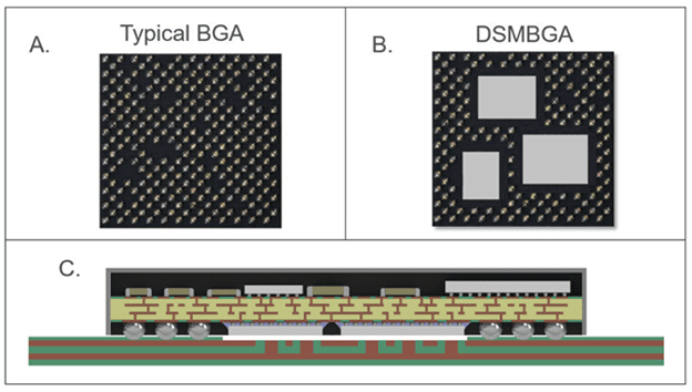
Figure 1: BGA layout difference between a typical BGA device (A) and a DSMBGA device (B) with active components and dies on the bottom side of the substrate. (C) Shows a representative cross-section of a DSBGA device
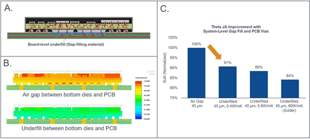
Figure 2: (A) Location of board-level underfill beneath dies on the bottom side of the substrate. (B) The simulation temperature difference between non-underfilled (top) and underfilled (bottom) packages. The color scale is consistent between images. (C) Simulation result chart with various underfill thermal conductivities
Case study 2: Large Body Package
The second case study in this presentation is a coupled structural-thermal simulation of a large body High-Density Fan-Out (HDFO) package with a central application-specific integrated circuit (ASIC) and multiple high bandwidth memory (HBM) modules (see figure 3). Most thermal simulations assume (for the sake of speed and simplicity) a constant thermal interface material (TIM) bond line thickness between the top of the ASIC/HBM module and the bottom of the lid. In this study, it was desirable to have a better understanding of how variations in bond line thickness (due to warpage) across the ASIC and module area could affect the thermal performance of the package.
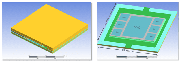
Figure 3: Large-Body HDFO Model. Quarter symmetry view (left). Expanded view (right) with lid hidden to show the ASIC+6 HBM HDFO module
A 63 x 63 mm HDFO package was first simulated in Ansys Icepak to generate a “power-on” temperature profile that could be applied to the structure in Ansys Workbench Mechanical. This temperature profile had two purposes: to apply as a temperature condition across the structural model to create stresses and calculate the deformation of the model due to the different coefficients of thermal expansion for each material; and second, to calculate a lid-top and substrate-bottom temperature boundary conditions to apply in the Ansys Mechanical steady-state thermal simulations of the deformed geometry and varied TIM bondline (see figure 4).
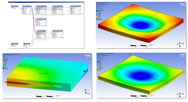 Fig. 4: (Clockwise, from top left) Ansys Project Schematic, showing linked subsystems that couple thermal and structural models. Package Warpage, 20°C, dead-bug view (looking at the bottom of the substrate). Package warpage with “Power-On” thermal gradient applied dead-bug view (same color scale as 20°C warpage). Temperature profile boundary condition as imported from Icepak
The deformed geometry (calculated at both 20°C for room temperature warpage baseline and at the Icepak-simulated “power-on” temperature) was then used as the geometry for thermal models. Variations of the active surface junction temperature, measured relative to an undeformed baseline, were calculated and reported across the die surface (see figure 5).
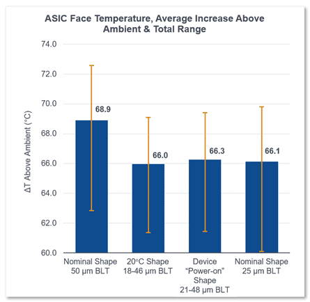
Figure 5: Temperature result chart of the various simulated ASIC temperatures. Error bars represent the total temperature range across the die face
Conclusions
The Ansys mechanical thermal model reports an average ASIC temperature of 88.9°C across the die face, with a maximum of 92.6° and a minimum of 82.8°C (for a temperature delta across the die of 9.7°C). The 20°C shape model reports 86.0°C average die temperature, a maximum of 89.1°C and a minimum of 81.4°C (for a temperature delta of 7.7°C across the die). The “Power-On” shape model reports 86.3°C average die temperature, a maximum of 89.4°C and a minimum of 81.4°C (for a temperature delta of 8.0°C across the die).
Die temperatures in the models that account for bond line thickness (BLT) variation appear to be more consistent (lower delta across the die) due to the thinner bond line at the center of the module and thicker bond line at the corners of the module (relative to a 50 µm BLT baseline). This case study results in a better understanding of the uncertainty of future models.
About the Author
Nathan Whitchurch is a senior staff engineer supporting packaging and mechanical simulation at Amkor. Prior to entering the electronics packaging field, Whitchurch worked on projects including vehicle-mounted computer rack enclosures, radio thermal design, data center thermal analysis, and systems integration. He provides system-level context and understanding of mechanical simulations at the package level. Whitchurch holds a BS degree in mechanical engineering from the University of Southern California.
Related Posts
Amkor Technology Launches Semiconductor Educator Bootcamp to Strengthen Future Workforce Pipeline

Amkor Showcases Next-Gen Packaging and U.S. Expansion at ECTC 2026