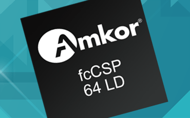
Smaller form factors with improved electrical performance
Amkor’s Flip Chip CSP (fcCSP) package – a flip chip solution in a CSP package format. This package construction partners with all of our available bumping options (Copper Pillar, Pb-free solder, Eutectic), while enabling flip chip interconnect technology in area array and, when replacing standard wirebond interconnect, in a peripheral bump layout. The advantages of flip chip interconnect are multiple: it provides enhanced electrical performance over standard wirebond technology, it allows for a smaller form factor due to increased routing density, and it eliminates the z-height impact of wire-bond loops.
The fcCSP package is assembled on a laminate or mold-based substrate with or without a core. The package is processed in a strip format for manufacturing efficiency and to minimize cost and enables bare die, overmolded and exposed die structures. The thermal challenges of high-power devices can be managed by applying an integrated heat spreader. Antenna in Package (AiP) can be enabled with the use of bottom side chip attach (POSSUM™). Finally, when coupled with copper pillar bumped die, fcCSP technology takes advantage of fine line/space substrate routing and bump pitch to reduce layer count and cost while increasing electrical performance.

The fcCSP package is an attractive option for applications in which both performance and form factor are critical. Examples include high- performance mobile devices (including 5G), infotainment and ADAS for automotive, and artificial intelligence. Further, the benefits from low inductance and increased routing density enable optimized electrical paths for high-frequency signals, making fcCSP suitable for Baseband, RF, and in-substrate antenna applications.
Features
- Suitable for low and high-frequency applications
- Low inductance of flip chip bumps – short, direct signal path
- No technological limitation to BGA ball count
- Target markets – mobile (AP, BB, RF, PMIC), automotive, consumer, connectivity, multi-die (side-by-side stacked) applications requiring high routing density
- Customer package sizes and shapes with strip-based processing
- Coreless, thin core, laminate, and molded substrate construction
- Bare die, over-molded, exposed die molded constructions
- Accommodates package sizes from 1×1 mm2 to 25×25 mm2
- Bump pitches down to 50 µm in-line and 30/60 µm staggered
- BGA ball pitches down to 0.3 mm
- Package thicknesses down to 0.35 mm
- Turnkey Solutions – design, bumping, wafer probe, assembly, final test
- Exposed die molding available for low-profile and thermal applications
- Heat spreader attach available for high-power devices
- Bottom-side chip attach available for Antenna in Package (AiP) applications (POSSUM™)
- Mass reflow and thermal compression chip attach available
Questions?
Contact an Amkor expert by clicking the request info button below.