
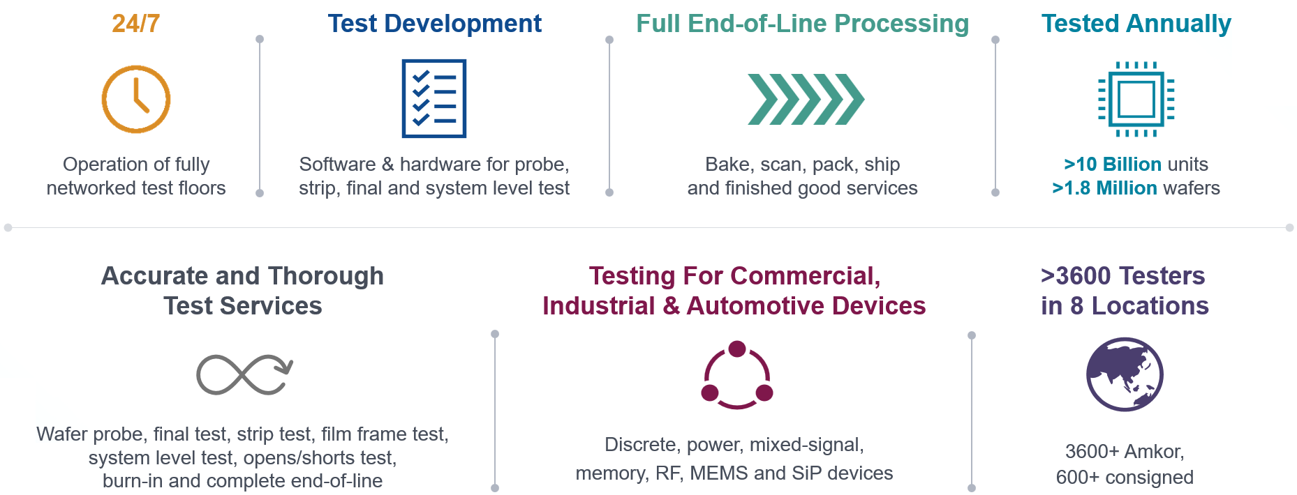
Innovative test solutions for diverse semiconductor system applications
With knowledge gathered from decades of supporting Tier 1 leaders and emerging industries, Amkor understands that test solutions must address advanced technology, quality, performance and cost of test. Through early engagement in each customer’s product lifecycle, Amkor helps define test strategies and intelligent equipment selection to provide differentiated test solutions.
Amkor offers comprehensive test services, including and not limited to, wafer level and package assembly. Amkor is the leading RF test services supplier engaged in ongoing joint efforts with test equipment suppliers and customers to enable 5G product production testing. As the top OSAT supplier for high performance compute (HPC), artificial intelligence (AI) processors & automotive testing, we have an extensive array of test capabilities and significant experience in device testing. The performance envelope for burn-in and system level test has recently expanded to account for higher power and lower cost.
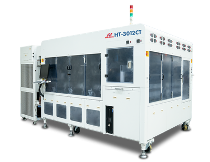
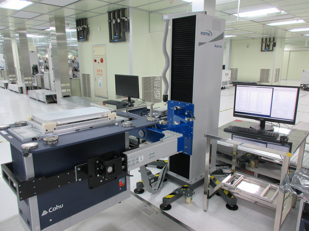
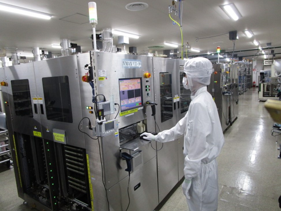
Test Equipment
Amkor has an extensive equipment fleet and continues to invest in new capabilities required to test the latest devices.
Application
- High performance compute, AI, power, memory, analog, RF, MEMS, sensor and SiP
Tester
- Clock: PEC clock rate, differential clocks, low Jitter, levels
- I/O: At-speed functional test. Low- & high-speed data I/O differential buses. Peripheral Event Controller (PEC) channel count, levels, timing – low EPA, patterns, test & measurements
- Power Delivery: Device power supply – channel count, levels, ganging, source and measure, high accuracy
- RF & Analog I/O: RF source & measure FE with optimal Rx/Tx port count to allow max parallelism for max UPH; ADC/DAC – resolution, accuracy, dynamic range to enable testing the latest technologies
- Optimal parallelism for max UPH
Load Board
- PCB material, PCB width, trace impedance
- Per pin current capability, pin-to-pin crosstalk
- RFID monitoring for tooling
- Temperature tolerance
Test Socket
- Per pin current capability, pin count per DUT, pin field planarity
- Pin-to-pin crosstalk/isolation/shielding
- Temperature tolerance
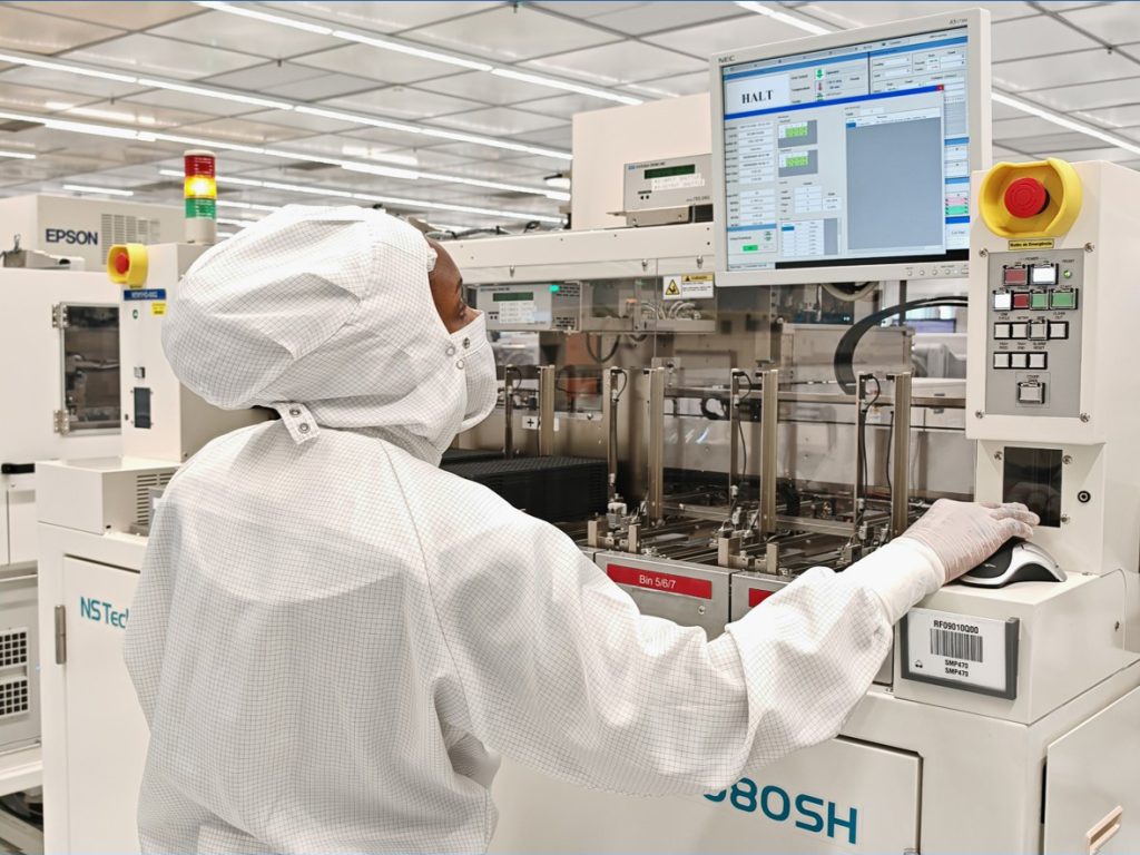
Handler
- Auto temperature control (ATC)/thermal soak
- Higher power up to 3200W (RM to 5000W)
- DUT rotation
- Footprint, contact force up to 650 kg (RM to 980 kg) loading force, loader speed
- Package handling, position XY accuracy
Application
- Die sales – Low-power apps
- Chiplets – 2.5D, 3D – μbumps, hybrid bonding
- Silicon photonics
Testers
- High-speed logic, mixed-signal, analog, high power and RF
- Probe pin data rate & current densities, economical parallelism
Prober
- Wafer Size – 8” and 12” with 7, 5, 3, 2 nm process technologies
- Chuck planarity, loading force, position XY accuracy, rotational angle
- Temperature range
- Reconstituted wafers
Probe Card
- All docking types e.g., cable, pogo tower, direct dock
- In-line LASER cleaning, overdrive
- Probe card technologies: Cantilever, vertical, pogo, membrane, MEMS & dual-level Chip on Wafer (CoW)
- Number of touchdowns
- Pin count per DUT, pin-to-pin crosstalk, per pin current capability
- Pin field planarity, alignment accuracy
Temperature tolerance
Application
- Logic, memory, and automotive
- Sub 30W, Up to 200W, Up to 1000W
- Wafer level & package level
- Massively parallel test insertion
Burn-in Tester
- High zone/chambers count
- Max clock rate
- Max I/O channel count
- Max slot count
- Product qualification & 100% burn-in support
- Wide power range
Burn-in Board
- DUT power delivery: All power application ICs supported
- I/O & clock rates supported
- Pin-to-pin crosstalk: Minimal for most, if not all, applications
- Socket config & features
- Cost-sensitive socket, with pin depopulation & biasing
- High temp tolerances
Burn-in Handler
- Burn-in Board (BIB) loader/unloader
Burn-in Loader/Unloader (BLU)
- All popular package types are supported
- High-efficiency input and output
- Manual component & BIB loading/unloading: Discouraged for higher volumes & 100% burn-in, in the interest of efficient cycle times
Application
- High performance compute, automotive, SiP
- Massively parallel test insertion
System Level Tester
- Clock Rate: High
- I/O: Max slot count, max I/O channel count
- Power Delivery: Range ultra-low, low, medium, high, rail count
- Max units per hour
System Level Test Board
- DUT power delivery – all power application ICs
- supported
- I/O & clock rates supported
- Pin-to-pin crosstalk – minimal for most, if not all, applications
- Socket configurations & features
- Cost-sensitive socket, with pin depopulation & biasing
- High temp tolerances
System Level Handler
- High test pattern zone count
- Product qualification & 100% support
- System level load/unloader
- All popular package types are supported
- High-efficiency I/O
- Temp controllers – low temp soak overhead times
Fully Customizable Backend Processes
- Post marking is optional and bake is determined based on the moisture sensitivity level (MSL)
- For small turret handler packages, the final test, scan and tape & reel packing is done sequentially
Advanced Solution for Advanced Packing
- Package-on-Package (PoP)
- Through Silicon Vias (TSV)
- Flip Chip CSP (fcCSP)
- Flip Chip BGA (FCBGA)

Test Locations
Our sites are strategically located near leading foundries, and major customer sites and co-located to support probe and test with assembly
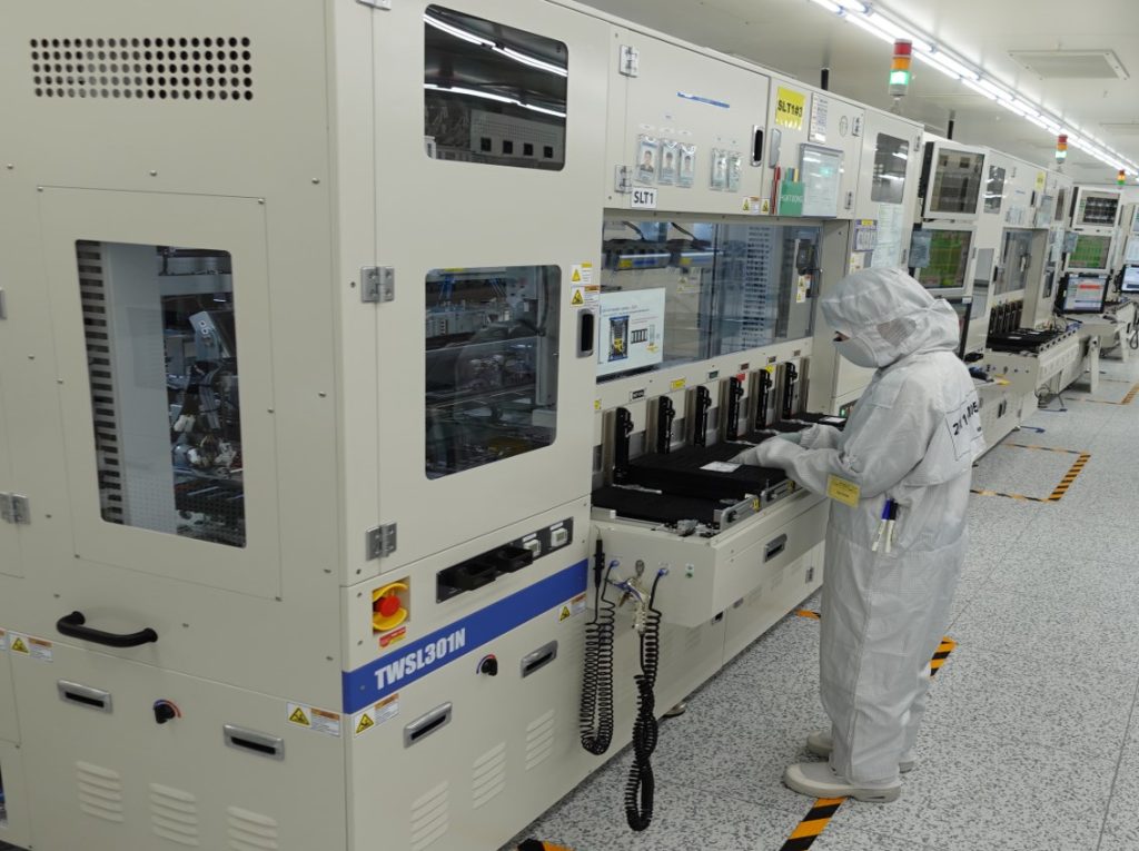
Amkor Technology Korea (ATK) operates strategic manufacturing facilities across South Korea, encompassing over 11M ft² of production space. Our facilities include advanced product development centers and comprehensive sales support offices positioned to serve key electronics manufacturing regions.
Our diverse technology portfolio includes stacked die, wafer level, MEMS, flip chip, Through Silicon Via (TSV), and 2.5/3D packaging solutions—enabling us to serve as a single source for complex semiconductor packaging needs.
With our ATK5 and ATK3 facilities located near Incheon International Airport and our ATK4 facility in Gwangju, we maintain efficient logistics capabilities that support quick turnaround times and seamless handling of large-volume orders for global customers.
Offerings
- Test development
- Wafer probe
- Package test
- Film frame test
- System level test
- Bumping
Packages
- FCBGA
- fcCSP
- MLF®
- TQFP
- TMV®
- TSV – 2.5D, 3D
- WLCSP
Markets
- High performance compute (HPC)
- Artificial intelligence (AI)
- Automotive
- Communication
- Consumer
Automation
- Autonomous Mobile Basket/Robot
- Socket cleaning
- Test program administrator
- Auto test program loading
- Auto yield monitor/data analysis/report
 Electrical Test
 System Level Test
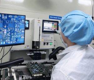 Test Hardware Repair Station
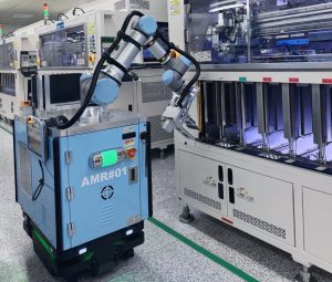 Autonomous Mobile Robot
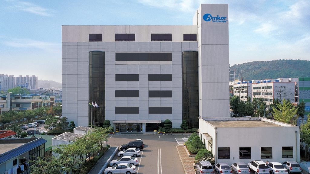 ATK3 – Incheon
 ATK4 – Gwangju
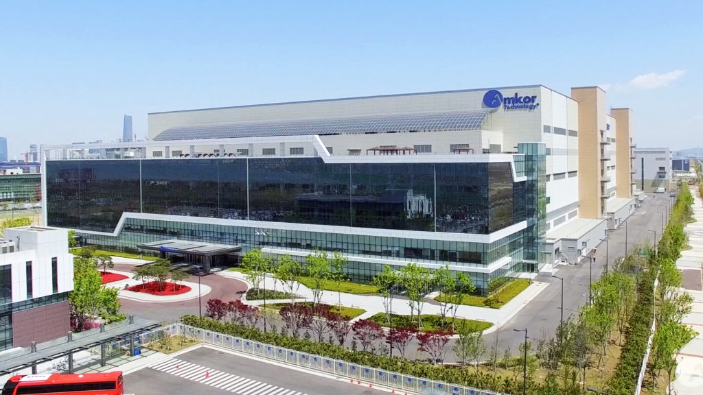 ATK5 – Incheon
Amkor Technology Taiwan (ATT) is situated in the HsinChu scientific area’s Taiwan Semiconductor Circle ecology, and it takes 30 minutes to reach the airport and wafer foundries. With Full-TurnKey solution services that include Bump/CP/WLCSP & Bump/CP/FCBGA/FT, Amkor Technology Taiwan (ATT) focuses on advanced packages (Bump, WLCSP and FCBGA). Additionally, ATT provides RD resources to help clients with complete solution design, including package, test program, and assembly development. ATT has 48,000 square meters of cleanroom manufacturing space.
Offerings
- Wafer probe
- Package test
- Film frame test
- Bumping
Packages
- Bumped wafer
- WLCSP
- fcCSP
- FCBGA
- SiP
Markets
- Communication
- Consumer
- Networking
 Final Test Tester
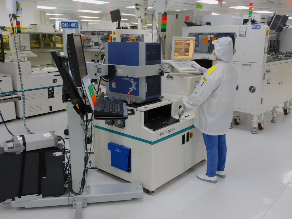
 Wafer Probe Test Cell
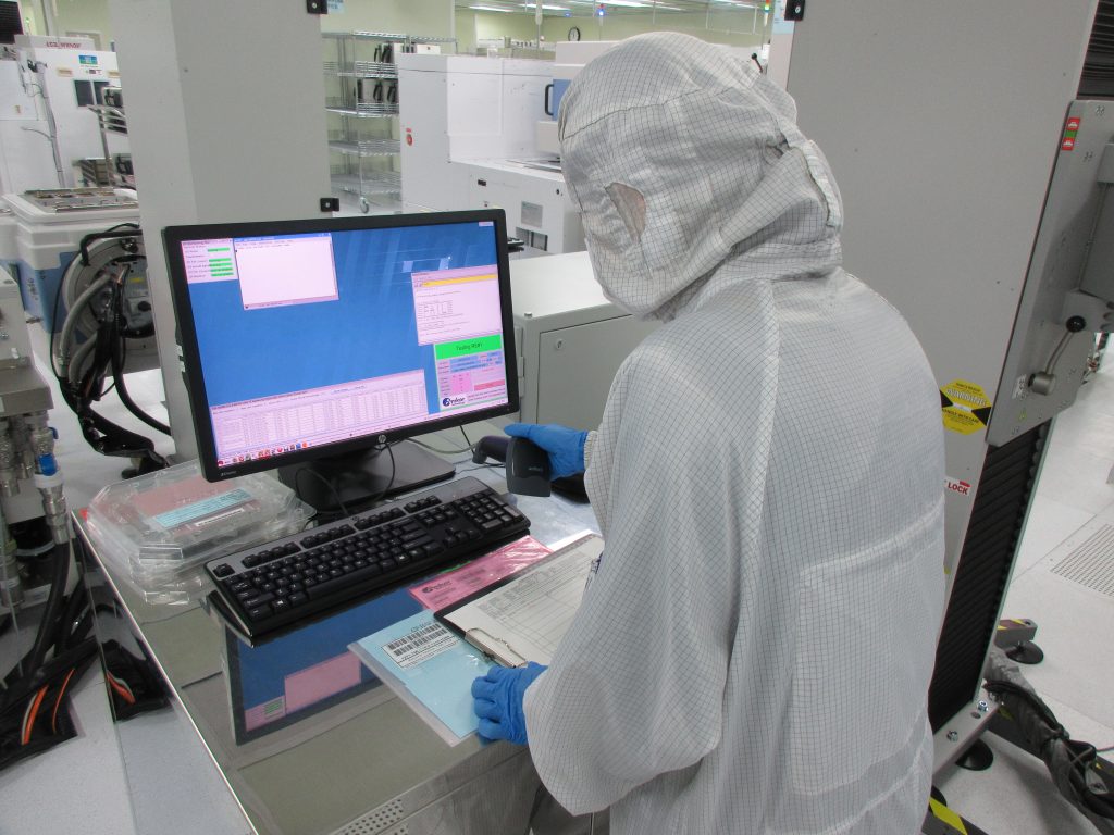 Operator Performing Lot Introduction
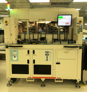 Final Test Handler
 ATT1 – Taoyuan City
 ATT3 – Hukou Township
 ATT6 – Taoyuan City
Amkor Technology Japan (ATJ) has seven factories and a head office. The head office is in Tokyo, which is only around 16 kilometers from HND airport and 5 kilometers from Tokyo Station. The factories are located all over Japan and the diversified manufacturing footprint is a key differentiator/competitive advantage that allows customers options to de-risk supply chains. ATJ has test experience with various semiconductor devices, e.g., mix analog, power discrete and module, System LSI and CIS and has 170,000 square meters of manufacturing space.
Offerings
- Wafer probe
- Package test
- Test development
Packages
- Flip chip
- PBGA
- Power discretes
- Power modules
- QFN
Markets
- Automotive
- Communication
- Consumer
- Industrial
 Burn-in Test Cell
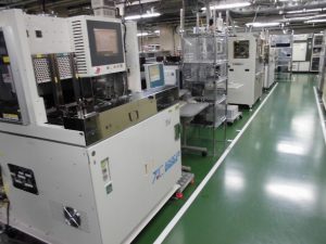 CCD Test Cell
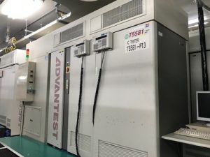 Memory Test Cell
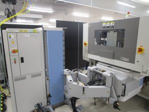 Final Test Cell
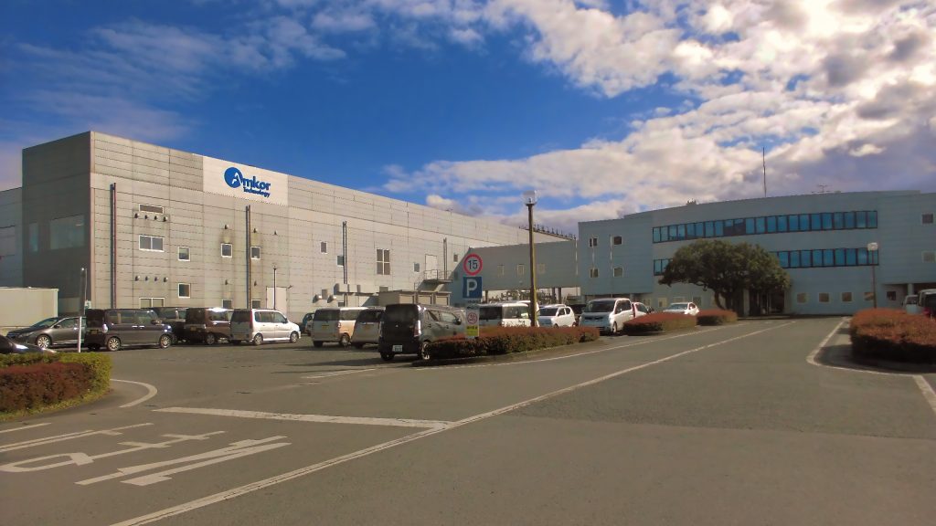 ATJ3 – Kumamoto
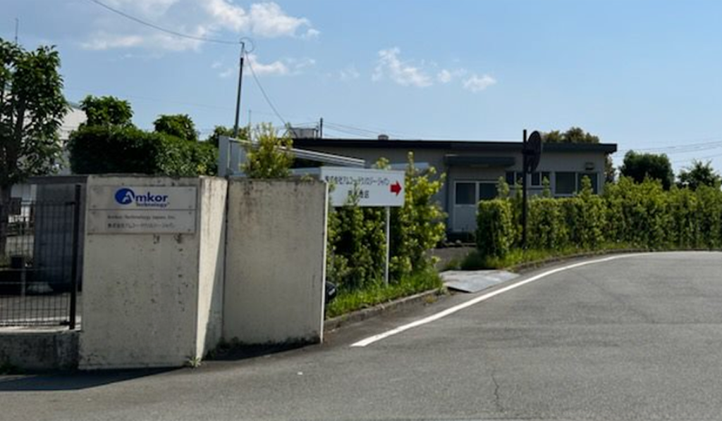 ATJ3 – Shisui
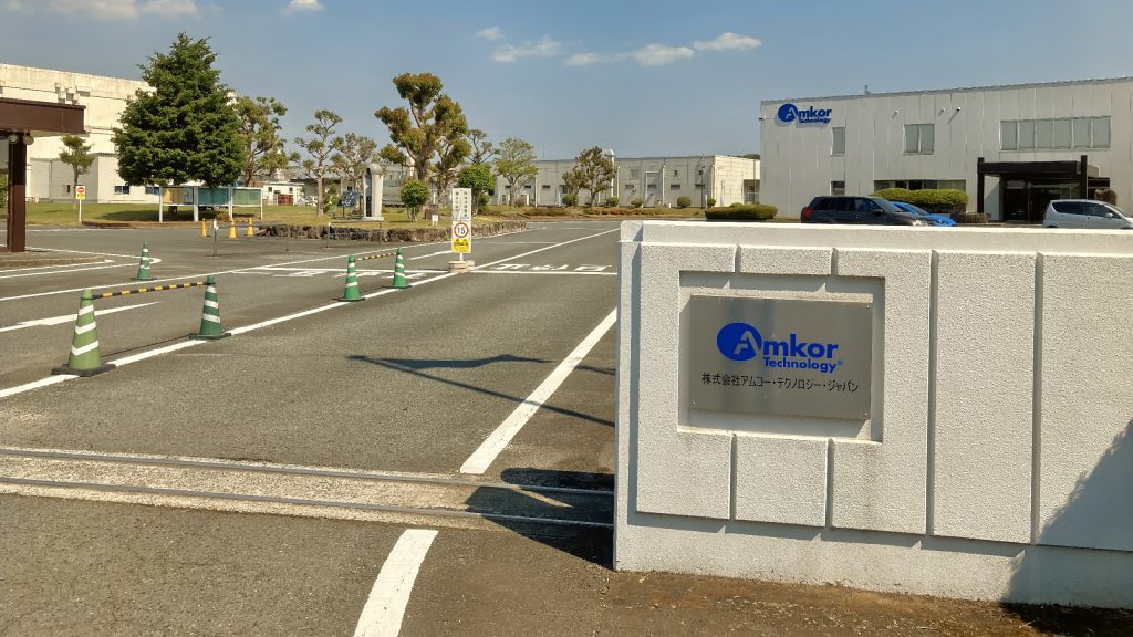 ATJ4 – Fukuoka
 ATJ4 – Kitakami
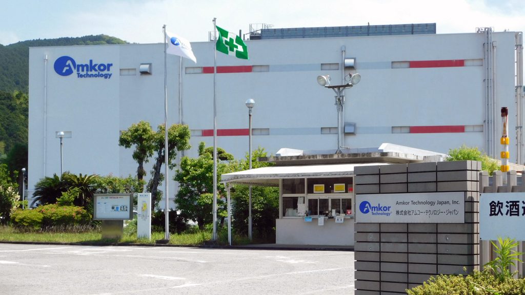 ATJ5 – Usuki
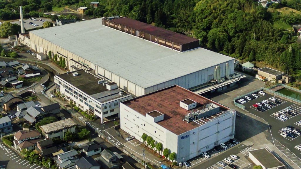 ATJ5 – Oita
 ATJ6 – Fukui
 ATJ7 – Hakodate
Amkor Technology Malaysia (ATM) is located in Malaysia’s Free Industrial Zone, about 50 kilometers from Kuala Lumpur city center and Kuala Lumpur International Airport. The Free Trade Zone’s convenient logistics and business-friendly policies allow Amkor customers to deliver goods around the globe through value-added taxes or tax exemptions. ATM has 32,000 square meters of manufacturing space and 108,800 square meters of land.
Offerings
- Package test
Packages
- SO8-FL
- SONXXX-FL
- TO-220FP
- TQFP
- TSON-FL
Markets
- Discrete
- Power
 End of Line (EOL)
 SO8 Package Final Test
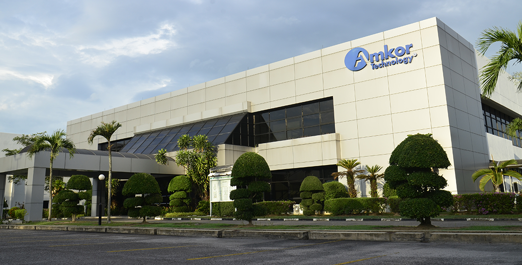 ATM1 – Malaysia
Amkor Technology Philippines (ATP) provides a full range of assembly and test services. ATP has two factories located in Muntinlupa City (P1) and Binan City, Laguna (P3/P4) to serve our global clientele. ATP P1, Muntinlupa City – has a manufacturing space of 32,000 sqm that is dedicated to producing legacy lead frame products.
ATP P3/P4, Binan City, Laguna, with a size of 32,800 sqm, is leading the way in advanced packaging technologies. P3 Assembly is recognized for its advanced packages and serves as a manufacturing and development center for MEMS and sensors. Amkor’s testing facility in P4 has been offering wafer probe and final testing services for the past 30 years, managing a wide range of applications including power and microcontrollers to MEMS.
With ATP registered with the Philippines Economic Zone Authority (PEZA), Amkor customers can enjoy significant benefits. The benefits consist of shipping products worldwide with incentives, VAT zero rating, and preferential tax rates, which guarantee a cost-efficient and efficient supply chain.
ATP has earned a reputation for its reliable packaging technology innovations and testing facilities. Our operational base encompasses both production and product development, which enables us to meet the changing demands of the semiconductor industry.
Offerings
- Wafer probe
- Package test
- Film frame test
- System level test
- Test development
- MEMS Test
- Burn-in
Packages
- MLF®
- Leadframe
- QFP
Markets
- Automotive
- Consumer
- Memory
 Wafer Probe
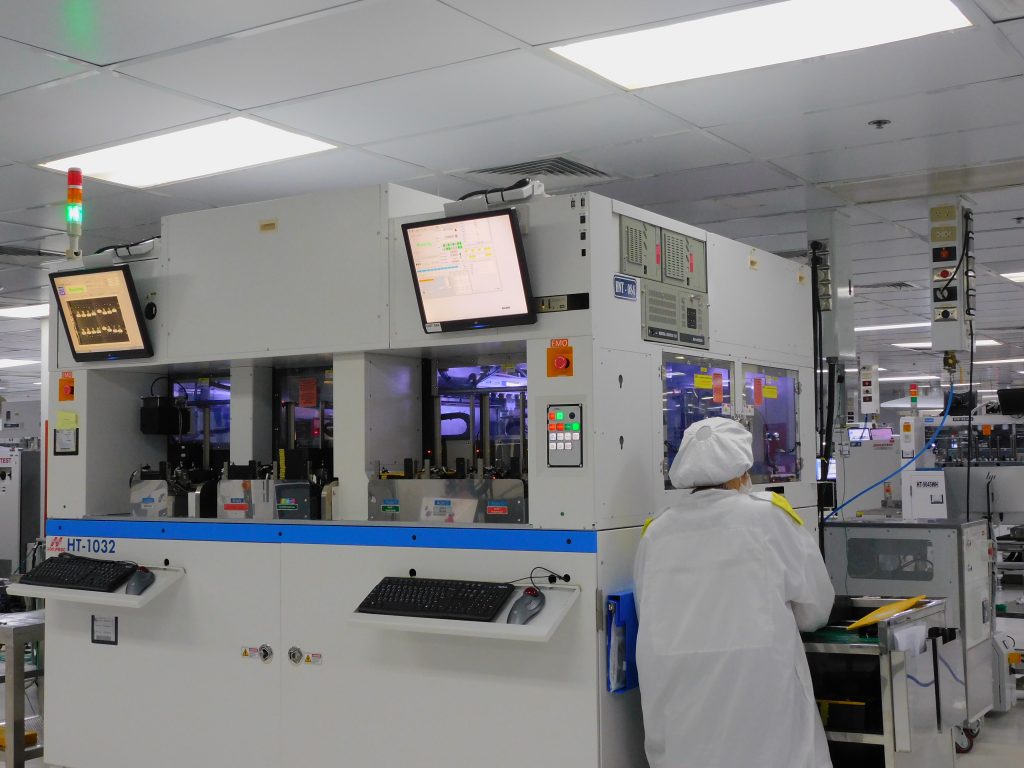 Final Test Pick & Place Handler
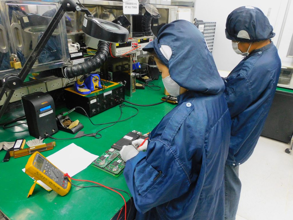 Test Hardware Repair Station
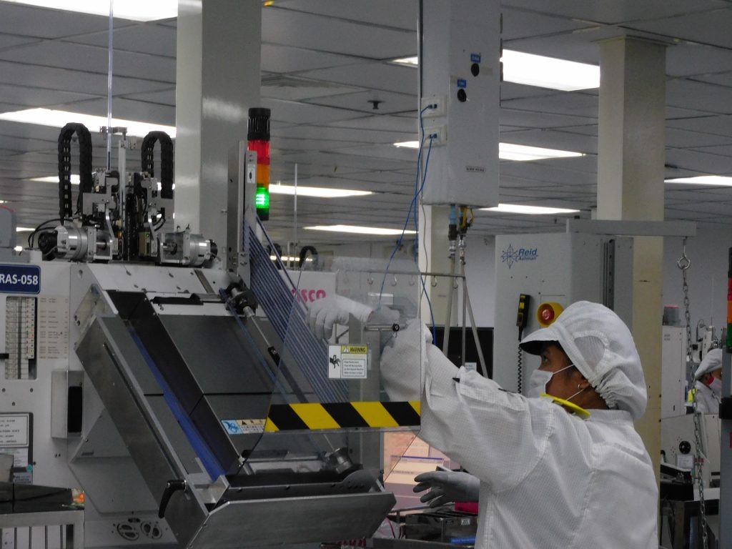 Final Test Gravity Feed Handler
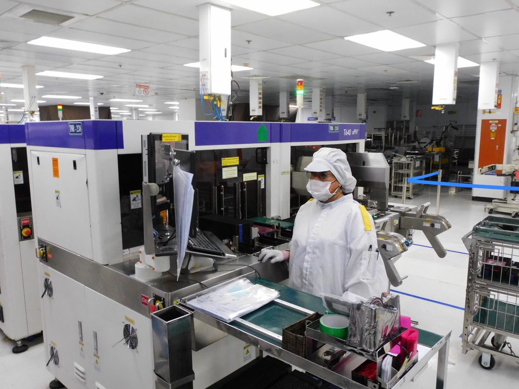 Post Test Tape & Reel Handler
 Burn-in Manual Load & Unload
 ATP3/P4 – Philippines
Amkor Technology Vietnam (ATV) is situated in Bac Ninh, and it takes 25 minutes to reach the airport. This site provides system in package and memory package and test services. Additionally, ATV provides RD resources to help clients with complete solution design, including package, test program, and assembly development. ATV has a large area of cleanroom manufacturing space.
Offerings
- Burn-in test
- Package test
- System level test
- Test development
- Wafer probe
Packages
- DPS
- SiP – DSMBGA
- SiP – DSLGA
- Stacked CSP
Markets
- Communication
- Consumer
- Memory
 SLT
SLT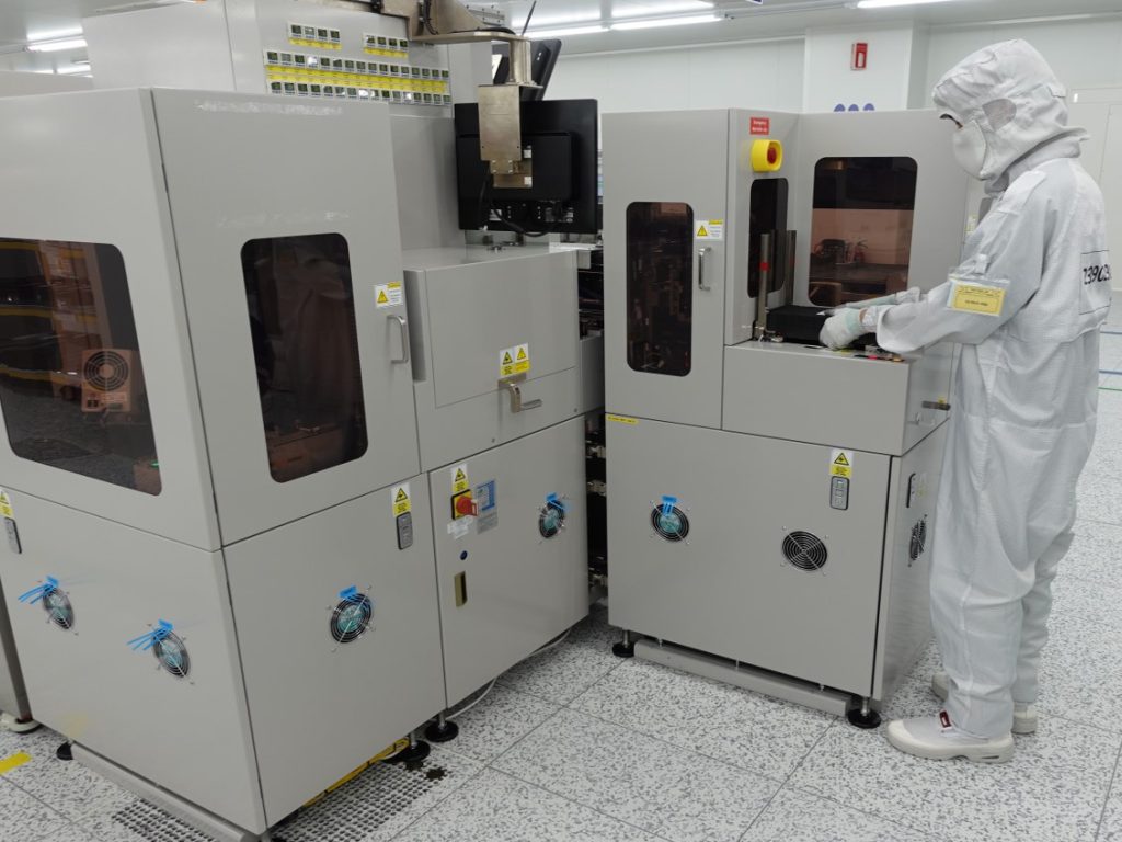 SCAN
SCAN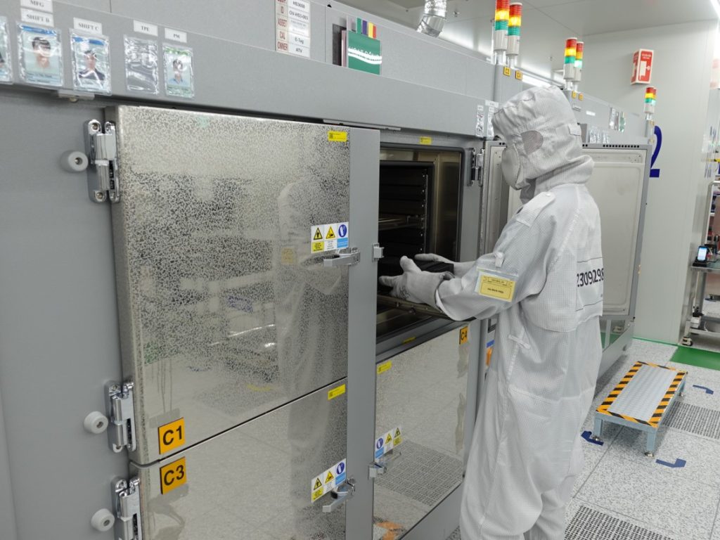 Bake
Bake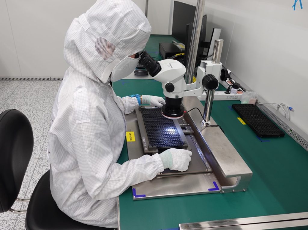 FVI Check
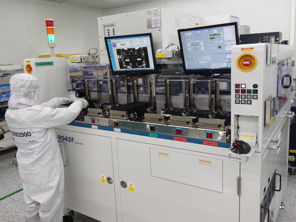 Final Test with Pick and Place Handler
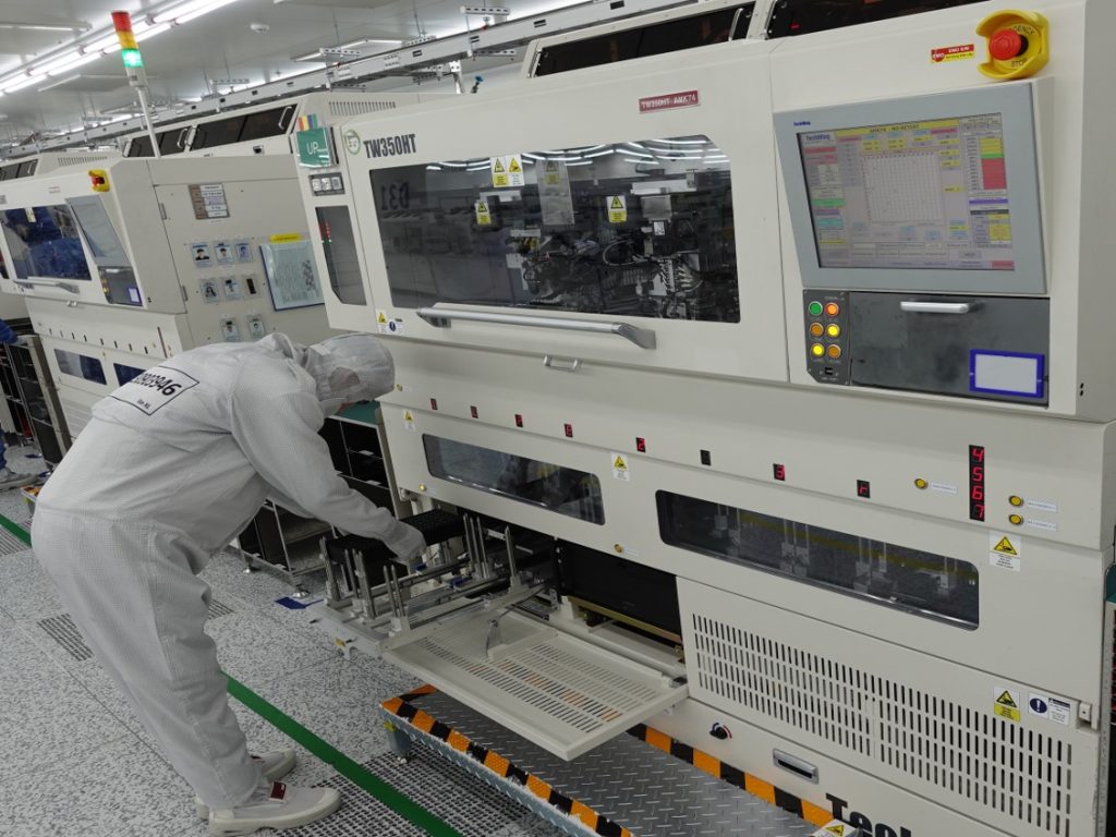 Memory Test Handler
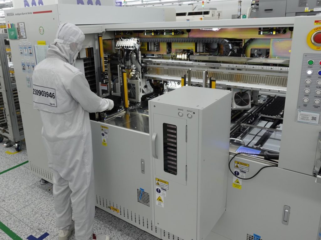 Memory Test Cell
 Test Hardware Repair Station
 ATV – Vietnam
Amkor Technology Portugal (ATEP) is located near Porto, the second biggest city in Portugal and fifteen minutes away from the international airport and seaport with excellent direct connections inside Europe and to the rest of the World. Being the biggest Outsourced Semiconductor Assembly and Test facility in Europe, dedicated to Advanced Packaging, the location benefits from accumulated semiconductor assembly and test experience in the region for more than five decades. ATEP currently has 20,000 square meters of clean room space and is expanding to 50,000 square meters.
Offerings
- Wafer probe
- Test development
Packages
- FCBGA
- WLCSP
- WLFO
Markets
- Automotive
- Communication
- Memory
 Opens & Shorts Test Handler
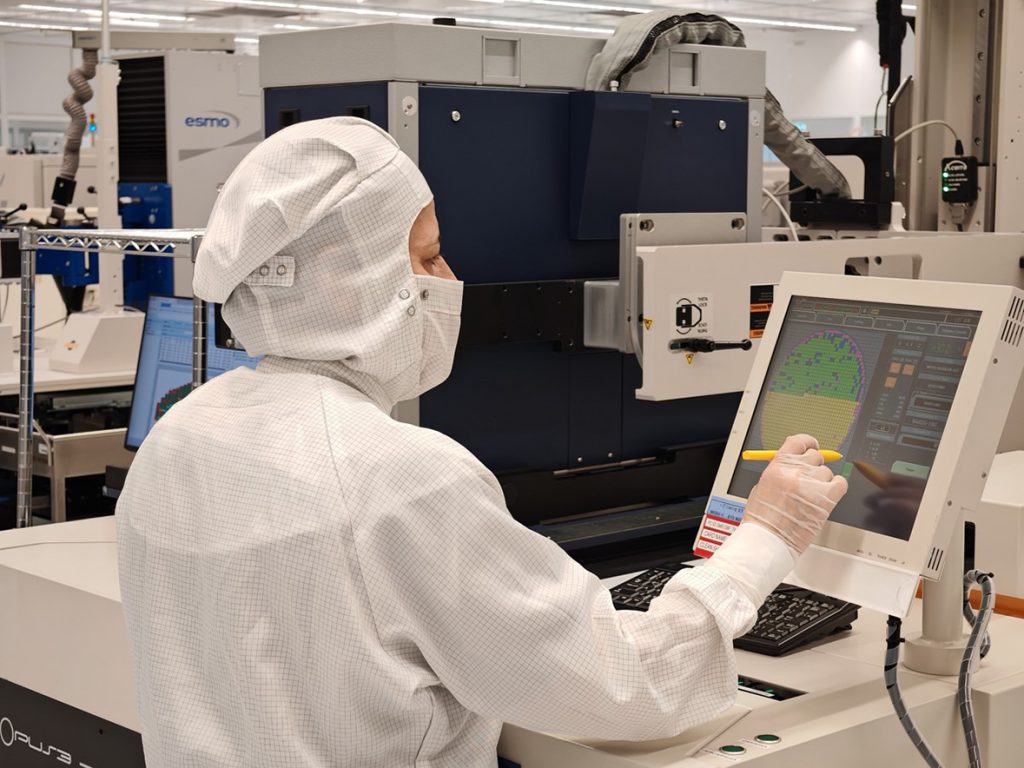 Cohu Tester
 Test Hardware Storage System
 Test Hardware Repair Station
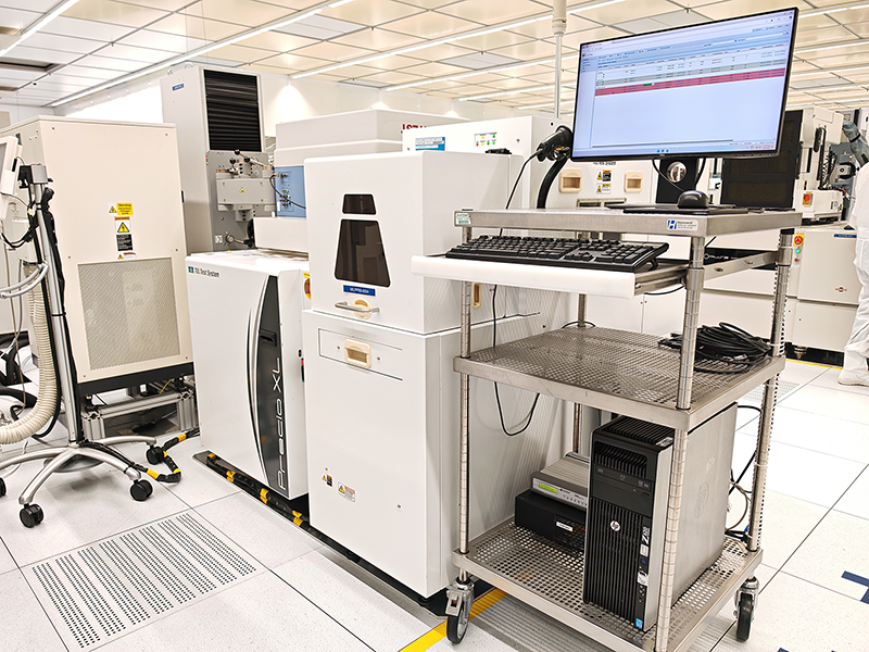 V93000 Wafer Probe Test Cell
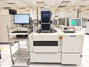 Cohu/Semics Wafer Probe Test Cell
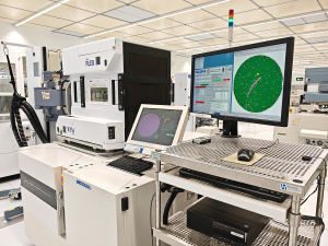 Ultraflex Wafer Probe Test Cell
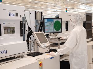 Ultraflex Wafer Probe Test Cell
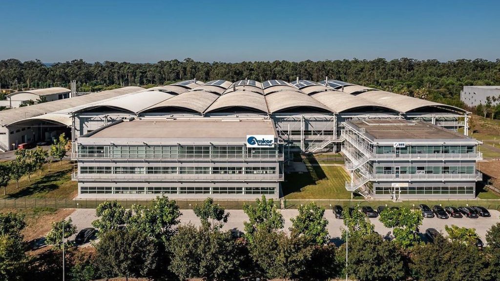 ATEP – Portugal
Amkor Technology China (ATC) is located in the Pilot Free Trade Zone, which is only about 30 kilometers from two primary airports in Shanghai. The Free Trade Zone’s convenient logistics and business-friendly policies allow Amkor customers to deliver goods around the globe through value-added taxes or tax exemptions. ATC has 170,000 square meters of manufacturing space.
Offerings
- Wafer probe
- Film frame test
- Package test
- Burn-in test
- System level test
- Test development
Packages
- CSP
- FCBGA
- Flip Chip
- MLF®/QFN
- PBGA
- WLCSP
Markets
- Automotive
- Communication
- Consumer
- Industrial
 Burn In
 Final Test
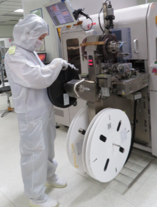 End of Line (EOL)
 Memory Test Cell
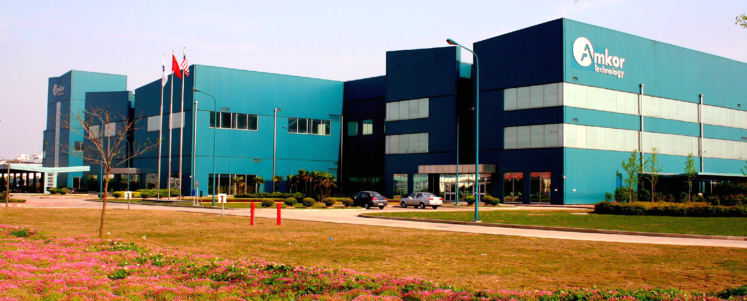 ATC1 – Shanghai
Test Development Engineering
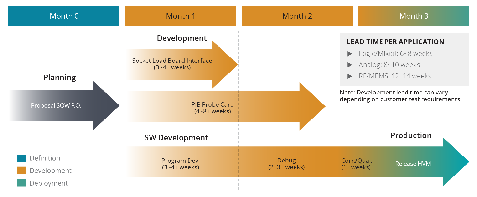
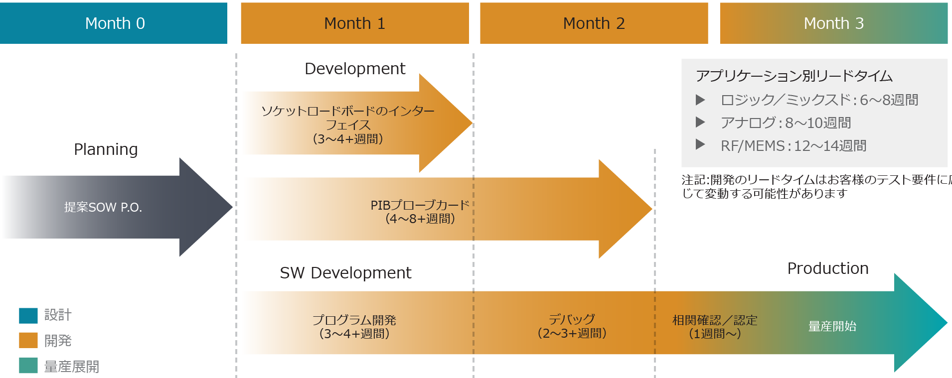
A fraction of customers develop their complete test solutions and outsource production to Amkor. Amkor can enable co-development, or full development, of complete test software and hardware solutions. Engage with us early in the product design for maximum impact or come to us later in the product lifecycle for significant cost savings with migrations to more cost-effective testers and/or higher parallelism.
Typical Test Development Cycle Times

Differentiated Test by Market
Amkor is the number one automotive OSAT, supporting worldwide supply chains. Products in this area include infotainment and safety (ADAS), requiring high levels of performance. This requires a comprehensive set of tests during the production test workflow.
- Cold wafer probe, room & hot temperature final test
- High-quality, standards-compliant processes and systems
- Inspections and multi-temperature test capabilities
- Wafer probe at -55°C to +200°C
- Final test at -55°C to +175°C
- Burn-in
- System Level Test (SLT)
- Cold wafer probe and perform room & hot temperature final test
- Post-assembly opens/shorts testing includes 2 and 4-wire resistance tests
The largest fraction of Amkor’s revenue is derived from the Communications market segment. This includes smartphones, tablets, handhelds and wearable devices. Our leading-edge test solutions keep pace with rapid changes in cellular and connectivity technology requirements. Amkor is well-positioned for 5G/6G RF wireless products and their test requirements.
- RF 5G NR conductive test for both FR1 and FR2 frequency ranges
- Asynchronous test for a multitude of RF connectivity standards
- ATE w/32 port and multi-site, multi-channel Tx & Rx support
- Complex SiP with simple SLT, including RF callbox testing
- Local RF shielding ≤60 dBm
- Multi-site x8 RF test to lower cost
- RF Front End (RFFE), SiP & IoT
- RF wafer probe capabilities – known good die (KGD) for WLCSP and known tested die (KTD) for SiP
- Single and multiple channel beamforming, phased array, AiP/AoP support
- SoC + Memory PoP – double side test/stack CSP – memory and logic test
Amkor is a leading provider of high-performance test solutions for the demanding networking and high-performance compute market. This market segment is driving the need for multiple chiplets that include artificial intelligence (AI) accelerators, central processing units (CPU), graphics processing units (GPU), field-programmable gate array (FPGA), input/output (I/O), serializer/deserializer (SERDES – PCIe, CXL), silicon (Si) photonics. Integral to these markets are advanced memory technologies like high bandwidth memory (HBM) and migrations from hard disk drives to solid-state drives (SSD), with NAND memories.
- Distributed test (wafer probe, in-situ test between key assembly steps and final test (SLT and ATE) for 2.5D & 3D). Probe solutions and wafer map management for chip-on-wafer (CoW)
- Active thermal control (ATC) for up to 300-watt & up to 1000W products across tri-temperature in SLT and ATE test
- Dynamic burn-in and test during burn-in (TDBI)
- Film frame and strip test (x308 EEPROM)
- High-speed serial digital (e.g. PCIe Gen4, Gen5) testing up to 16 Gbps and 32 Gbps
- Silicon photonics ICs
Amkor is a leader in power discrete devices & modules like diodes, flip chip MOSFETs, intelligent power modules, Insulated-Gate Bipolar Transistors (IGBT), multi-voltage FETs, regulators and bipolar transistors for the automotive, power transmission and industrial segments. Amkor’s test services are closely integrated with the assembly flow for shorter cycle times and reduced costs. Key characteristics include:
- High current, high voltage
- Kelvin contact-type tests
- Low Rds_on
- Si, SiC, Gan
Products for today’s Internet of Things (IoT) and Industrial Internet of Things (IIoT) require an MCU, RF transmitter/receiver, sensors and actuators. Sensor technologies include and are not limited to magnetometers, accelerometers, gyroscopes, proximity, RF switches, photo sensors, microphones, micro-speakers, humidity, pressure, and temperature. The test solution needs to cover the conversion of these physical, real-world analog signals in a variety of range of operations into an electrical stimulus that is tested during the production workflow.
Questions?
Contact an Amkor expert by clicking the request info button below.