Leaders in wafer bumping and die-level interconnect technology
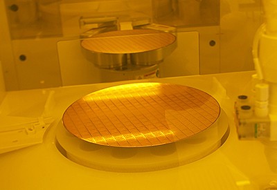
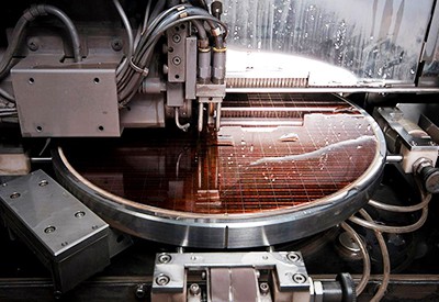
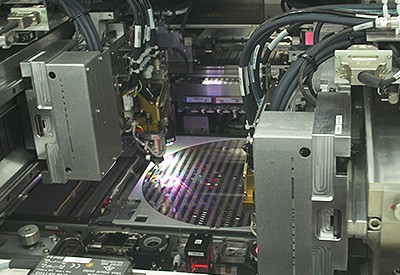
Amkor’s production-certified wafer bumping processes and die-level interconnect technology is unparalleled in the industry, offering reduced time-to-market with integrated factory logistics. Amkor maintains strong initiatives in the area of technology development to further support customers’ future needs. Continuous improvement programs are in place to optimize and cost-reduce wafer bumping processes.

Amkor’s state-of-the-art wafer bumping capabilities in electroplated bumping and various types of Wafer Level Chip Scale Packaging (WLCSP) in multiple strategic locations. Our China, Korea, Portugal and Taiwan bumping operations are co-located with wafer probe, assembly and final test, enabling Amkor to provide complete “turnkey” flip chip and WLCSP solutions in these key geographic locations.

All Amkor facilities have world-class bumping lines with high-volume manufacturing (HVM) production capability. 200 mm and 300 mm lead-free and Cu pillar solder compositions (all low alpha) are production certified. Service offerings include repassivation and single and multi-layer redistribution processes for both flip chip and WLCSP applications.

These facilities offer economy of scale as both plated bump (solder/CuP bump) and WLCSP/Wafer Level Fan-out (WLFO) continue to grow. This combination of technology and manufacturing capabilities is unparalleled in the subcontract manufacturing industry. In addition, Amkor facilities are situated adjacent to major foundry sources and provide customers reduced time-to-market with integrated factory logistics.
Questions?
Contact an Amkor expert by clicking the request info button below.