Will An Adhesion Promoter Prevent Delamination in Power Semiconductor Packages?
Power semiconductor packages are used in high-temperature, high voltage environments. With the increase of electric vehicles (EVs) and hybrid electric vehicles (HEV) in the automotive market, demands on (and for) power packages have been growing. Packages for automotive applications must pass extensive testing for safety, therefore, packaging reliability is essential. As more power semiconductor packages are used in automotive applications, it is increasingly important the package has zero delamination.
Challenge of Delamination-free Semiconductor Power Packages
Semiconductor packages consist of several different materials. Each material has a different property, such as its coefficient of thermal expansion (CTE). With these different properties, passing extreme testing and achieving a real “zero delamination” is a challenging task for semiconductor manufacturers.
There are four major interfaces for a typical power package structure. The D2PAK (TO-263 as the JEDEC standard) package provides an example of these interfaces (Figure 1 and Figure 2). Designed for low on-resistance and high-speed switching MOSFETs, the D2PAK is suitable for high-power applications. It is used in motor drivers, power supply circuits and DC-DC converters.
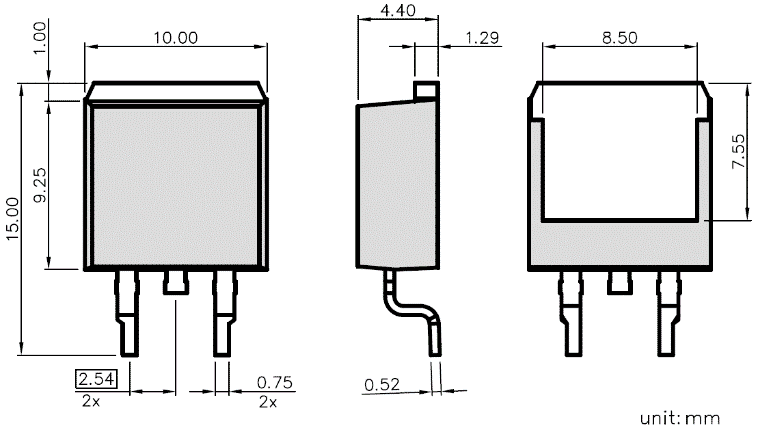
Figure. 1: Package outline drawing of D2PAK.
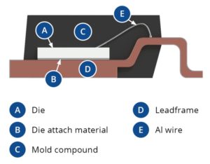
Figure. 2: Cross-section of D2PAK.
The standard materials of a D2PAK are bare copper (Cu) leadframe (LF), solder (die attach), aluminum (Al) wire (interconnect) and an epoxy mold compound (EMC) for encapsulation. The material of the die can be silicon (Si), silicon carbide (SiC), or gallium nitride (GaN). The different types of materials require strong adhesion to each other to withstand severe environment reliability testing and pass the safety standards for an automotive component.
Delamination could occur between EMC and copper LF, EMC and lead (Pb) solder, EMC and Al die pad and/or EMC and nickel (Ni) lead pad (figure 3).
The weakest adhesion point is between the EMC and the solder. The development goal is to achieve zero delamination at T=0 (after moisture resistance testing (MRT))*¹ and the temperature cycle (TC)*² 2000x.
*¹MRT: JEDEC Lv. 1 (245°C reflow x 3)
*²TC condition: -55°C to 150°C
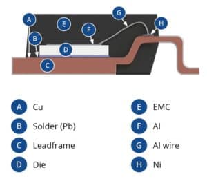
Figure 3: Surfaces of possible delamination.
Effectiveness of Adhesion Promoter
The material selection for an adhesion promoter (AP) is very important because it must be compatible with mold resin, copper, aluminum, nickel and Pb solder. Several polyimide bases and epoxy-based materials were selected for the evaluation. First, the adhesion strength was tested by the cup-shear test (Figure 4).
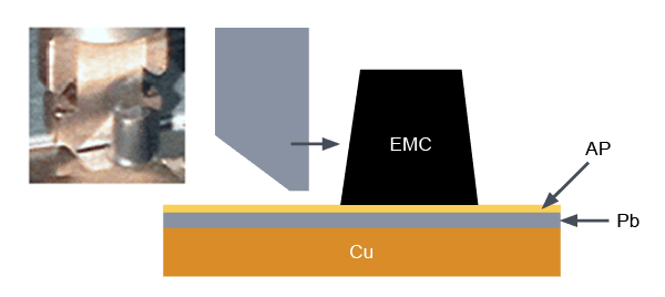
Figure 4: Adhesion strength measurement by the pudding cup-shear test.
All the AP materials showed an increased adhesion strength vs. the non-AP coated surfaces at both room temperature (RT) and 150°C (figure 5).
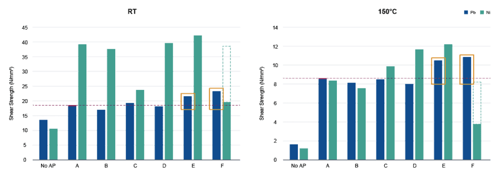
Figure 5: Adhesion strength comparison.
After the initial test, the adhesion promoters were tested on a package, using the D2PAK as a test vehicle. The AP was coated with a jet dispenser after wire bonding to cover the bonding area (Figure 6). Also, different types of EMCs were used for comparison.

Fig. 6: The process flow from die attach to trim & form (TF) including adhesion promoter coating.
The design of experiments (DOE) was conducted with a non-AP coated package as a reference and three AP materials with different EMCs. The scanning acoustic tomography (SAT) inspection was performed at initial, MRT (MSL 1), TC 500x TC 1000s, TC 1500x and TC 2000x. The package with the AP2 coating survived TC 2000x and achieved perfect zero delamination (figure 7 and figure 8).
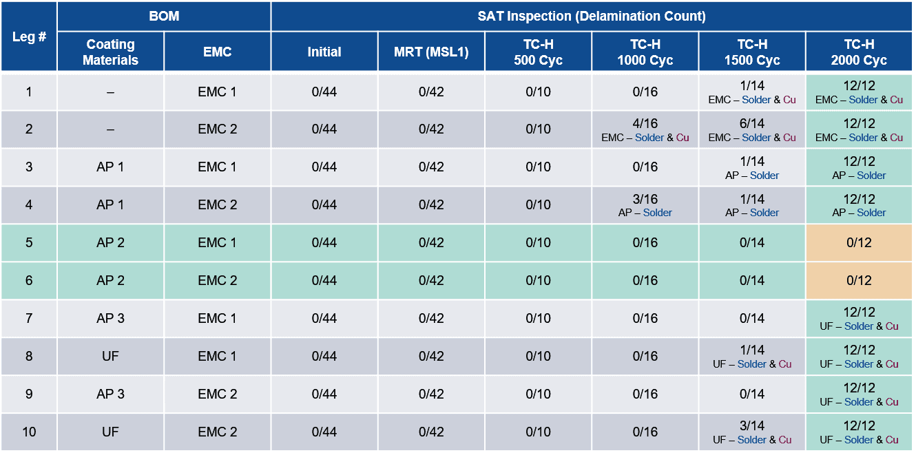
Fig. 7: Temperature cycle test result of AP coated package DOE.

Fig. 8: SAT inspection of test samples.
The results to date are promising to enhance package reliability levels by adding an adhesion promoter in the assembly process to achieve zero delamination. It is also worth mentioning that implementing the AP coating is cost-effective since it can be applied by a dispensing tool that is already used at most assembly sites.
Conclusion
One of the AP materials achieved perfect zero delamination at TC 2000x on all interfaces. We identified the key material properties to be used as a good adhesion promoter. The next development target is to expand the AP to other packages and another structure, such as power packages with a Cu clip structure.
About the Author
Sophie Olson is Sr. Manager, Wirebond and Power Package Development at Amkor Technology. She joined Amkor in 2004 and is currently responsible for the development of power packages and semiconductor packaging materials. Before joining the R&D team, she spent two years at Amkor Japan to help expedite the integration of Amkor subsidiaries. She previously held business operations, sales and customer service roles as well. She holds a BA in Materials Science and Engineering from Arizona State University and a master’s degree in Political Science from FSU.
