Achieving Success in Automotive Leadframe Packages
The growth of semiconductor content in automotive applications has been accelerating. This growth drives all families of semiconductor packaging in all regions. The growth is happening in the latest advanced, laminate-based packages using flip chip interconnect as well as the venerable leadframe packages using wirebond interconnect. The automotive market consumes micro-electromechanical systems (MEMS) packages as well as leadframe packages such as Quad Flat Pack (QFP) and Small Outline Integrated Circuit (SOIC) packages and the fast growing MicroLeadFrame® (MLF®)/Quad Flat No-Lead (QFN) packages. Increasingly, the industry depends on Outsourced Assembly and Test (OSAT) suppliers to provide wire bond leadframe packaging support.
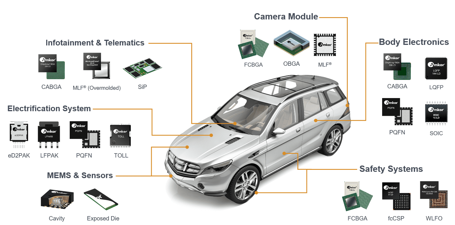
In addition to growth, the quality and reliability requirements of the automotive market have increased significantly. Among other things, automotive customers demand zero defects and zero delamination after extended reliability testing. To achieve success with automotive leadframe packages, Amkor has invested and continues to invest substantial resources in two strategic directions.
Automotive Process Enhancements
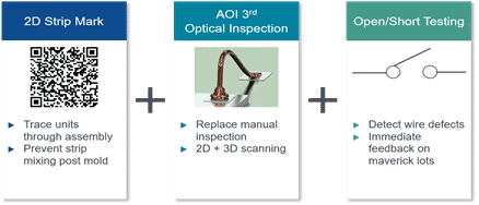
The first strategic direction is the development of automation tools to significantly reduce escaped defects. Defect trapping/isolation has been improved by marking tracking identification on leadframe strips prior to the start of assembly. The tracking marks are then used to create defect maps when automatic optical inspection (AOI) is performed following wire bonding and again during sample open and short (O/S) electrical testing after the completion of assembly. In addition to preventing defective parts from escaping, these automatic inspections provide rapid feedback to the process engineering team in the factory. In the case of the defects caught at AOI, there is a photographic record of all defects found that the engineering team can use to troubleshoot the issue without the need for further failure analysis. Customers are reporting an increase in their final test yield as assembly-related defects are screened out. After a decrease in yield when AOI and O/S were initially introduced, the fast feedback supports ongoing assembly continuous improvements by leveraging the customer feedback provided.
 Defect Trapping/Isolation
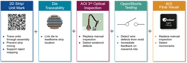
As a part of the plan for extending the implementation of automation for the automotive market, Amkor is currently developing support for Die Traceability Systems (DTS) for leadframe products as the first step towards Unit Level Traceability (ULT). DTS leverages the equipment and processes put in place to support defect trapping (2D marking, AOI at third OP and O/S) with the addition of integration of the die attach equipment with the strip mark tracking to link the customer electronic wafer map to leadframe strip maps. This creates a record of which die are placed on which leadframe locations. Unit laser markers near the end of the assembly process then mark a 2D code on the package identifying the package and linking it to the information about the die and wafer as well as the defect maps generated during the assembly process. DTS records will be electronically transferred to customers as needed. Once support for DTS has been completed, Amkor will expand the strip level traceability and mapping over time to all other assembly process stations to eventually be able to provide ULT.
Standard Product Definitions for Automotive
The second strategic direction has been the development of the capability for leadframe packages to consistently achieve zero delamination following extended automotive reliability (AEC Q100 & Q006 G1 & G0) testing. Many different combinations of processes and materials were tried before consistent results were achieved. With the initial success of these efforts, further implementation is occurring across the broad portfolio of leadframe packages. This success has been achieved by focusing on many factors including design, process, and environmental controls, as well as the interactions of physical properties of the bill of material (BOM) elements. The design features that have been developed are based on a proprietary understanding of how to incorporate mold locking features along with the relative dimensions of key features including the plating of noble metals.
 Die Traceability Systems (DTS)
Robust Design Features Supporting Automotive
 Edge ProtectionTM Technology + Dimples
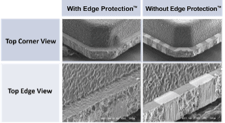
Edge ProtectionTM Technology for pMLF® Packages
Amkor also has worked with our key material suppliers to develop proprietary die-attach and mold compound formulations with matched physical properties. We have also developed an in-depth understanding of our leadframe suppliers plating and roughening capabilities so that we can source the best solutions for automotive applications. Based on all these studies, Amkor has developed Standard Product Definitions (SPD) by package family which defines the recommended BOM and process flow for packages that will be deployed in demanding environments such as many of those in the automotive market. The investment of significant resources in various areas has led to achieving success in the automotive leadframe marketplace.
About the Author
John Nickelsen joined Amkor in 1995 and is currently the VP of Product Engineering for leadframe products, with a focus on improving quality and yield while reducing cost for leadframe products. He previously managed the Dual Leadframe products team, and the microEMS product group and was a member of the Concentrated Photovoltaic package development team. Prior to joining Amkor, John worked for ASE and Motorola. He holds a bachelor’s degree in Mechanical Engineering from the University of South Florida and a master’s degree in Engineering from Florida Atlantic University.
