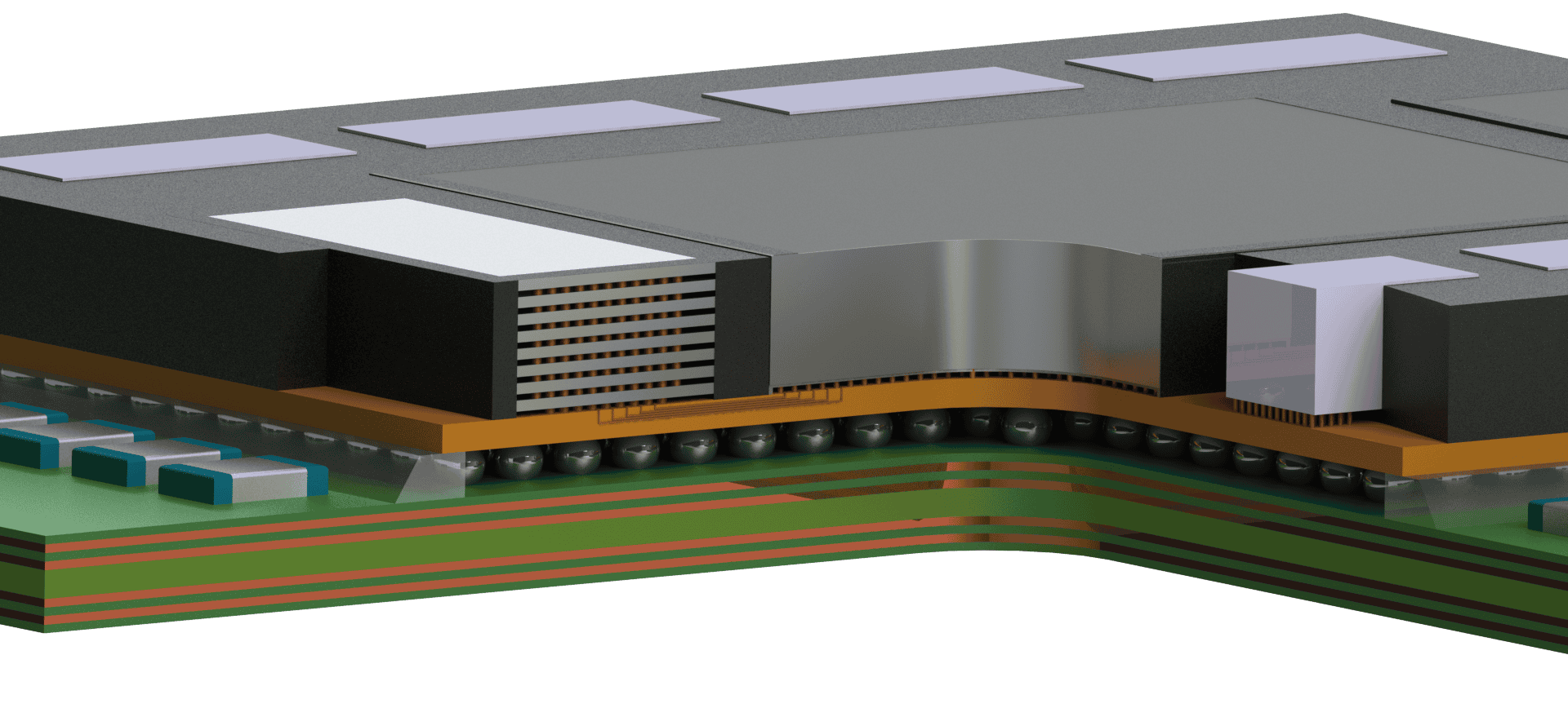
S-SWIFT is a revolutionary new packaging technology
Substrate-SWIFT (S-SWIFT) technology, also known as Silicon Wafer Integrated Fan-Out (on Substrate), is revolutionizing the world of advanced packaging. By boosting I/O and circuit density while shrinking the footprint and profile, S-SWIFT is the go-to solution for both single-die and multi-die applications, perfectly aligning with the escalating demand for higher IC integration in mobile and networking devices.
S-SWIFT stands out as a game-changer in heterogeneous IC packaging, enabling high-performance, cost-effective integration of multiple chiplets and memories. This technology not only increases I/O and circuit density but also paves the way for advanced 3D structures, making it indispensable for the next generation of mobile and networking applications. S-SWIFT technology is well-suited for applications that require large package sizes and high I/O density (>1000).
Fan-Out Meets Substrate
An innovative alternative to 2.5D TSV, S-SWIFT is a fan-out package that enhances chip performance and reduces costs. By flip-chip mounting chips onto a high pin count ball grid array (BGA) substrate, and incorporating a re-distribution layer (RDL) for shorter die-to-die (D2D) interconnections, S-SWIFT treats the entire fan-out package as a single die. This intelligent design is then mounted onto the BGA substrate, offering a cost-effective alternative to traditional 2.5D Through Silicon Via (TSV) technology.
A key feature of S-SWIFT is its RDL, which enables shorter D2D interconnections between multiple chips. This design treats the entire fan-out package as a single die, then mounted onto the BGA substrate. By integrating these advanced features, S-SWIFT offers a cost-effective alternative to traditional 2.5D TSV technology.
Package Structure
- Fan-out package flip-chip mounted on a high pin count BGA substrate
- RDL facilitates shorter D2D interconnections between multiple chips
Chip Integration
- Integrates multiple chiplets within a single package
- Chiplets can be different functional units, such as ASICs or HBMs
Interposer-less Design
- Eliminates the need for an interposer, reducing complexity and costs
Electrical Performance
- Offers excellent electrical performance due to shorter D2D connections
- Features less insertion loss, better impedance control, and lower warpage
High I/O Density
- Supports high I/O counts (>1000)
- Ideal for large package sizes and networking/server applications
- Cost-effective: Eliminates the need for an interposer, reducing package costs
- Electrical Performance: Offers better impedance control, lower insertion loss, and less warpage, resulting in improved electrical performance
- High I/O Counts: Supports packages with over 1000 I/Os, making it ideal for networking and server applications
- Time to Market: Leveraging existing fan-out/flip chip techniques, this technology accelerates time to market
S-SWIFT™ technology offers lower costs compared to 2.5D, a thinner package, reduced insertion loss, improved impedance control, and lower warpage, resulting in superior electrical performance. These advantages make S-SWIFT a compelling choice for relevant applications.
Key applications include:
- High Performance Computing (HPC): Enhances HPC applications by efficiently achieving critical interconnections
- Networking and Server Applications: High I/O density makes S-SWIFT ideal for networking and server needs
- Artificial Intelligence (AI): Exceptional electrical performance and high-speed, low-latency chip-to-chip interconnect are perfect for AI applications requiring significant memory and compute power
- ASICs and HBMs: The chip-last technology of S-SWIFT is suitable for packaging ASICs and HBMs


Questions?
Contact an Amkor expert by clicking the request info button below.