
S-SWIFT, 새롭고 혁신적인 패키징 기술
서브스트레이트 상의 실리콘 웨이퍼 집적 팬아웃이라고도 불리는 S-SWIFT(서브스트레이트 SWIFT) 기술이 첨단 패키징 분야에 혁신을 불러일으키고 있습니다. S-SWIFT는 면적을 줄이고 조도를 낮추면서 I/O와 회로 밀도를 높인다는 점에서, 단일 다이와 다중 다이 애플리케이션에 모두 적합한 솔루션이고 모바일 및 네트워킹 디바이스 영역에서 증가하는 IC 통합 수요에 완벽하게 부합합니다.
S-SWIFT는 여러 칩렛과 메모리를 뛰어난 성능과 높은 비용 효율로 집적할 수 있게 함으로써 이기종 IC 패키징에서 독보적인 기술로 존재감을 과시합니다. I/O와 회로 밀도를 높이고 첨단 3D 구조를 위한 기반을 마련하여 차세대 모바일 및 네트워킹 애플리케이션의 필수로 자리잡고 있는 S-SWIFT 기술은패키지 사이즈가 크고 I/O 밀도가 높아야 하는(1000 초과) 애플리케이션에 잘 맞습니다.
팬아웃과 서브스트레이트의 만남
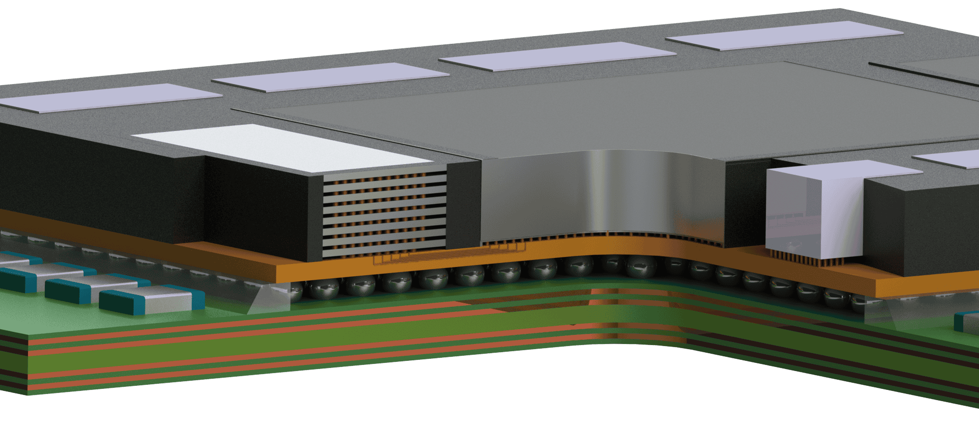
2.5D TSV를 혁신적으로 대체하는 S-SWIFT는 칩 성능을 높여주고 비용은 낮춰주는 팬아웃 패키지입니다. S-SWIFT는 하이 핀 카운트 볼 그리드 어레이(BGA) 기판에 칩을 플립칩으로 실장하고 다이 대 다이(D2D) 인터커넥트가 짧아지도록 재배선 레이어(RDL)를 집적하여, 팬아웃 패키지 전체를 단일 다이로 처리합니다. 또한 이 지능형 설계를 BGA 기판에 실장하여 기존 2.5D 실리콘 관통전극(TSV) 기술을 비용 효율적으로 대체합니다.
S-SWIFT의 핵심 기능은 여러 칩 간의 D2D 인터커넥트를 단축시키는 RDL입니다. 이는 팬아웃 패키지 전체를 단일 다이로 처리한 뒤 BGA 기판에 실장하는 설계 방식이며, S-SWIFT는 이렇게 첨단 기능들을 통합하여 기존 2.5D 실리콘 관통전극(TSV) 기술을 비용 효율적으로 대체합니다.
패키지 구조
- 하이 핀 카운트 BGA 기판에 팬아웃 패키지 플립칩 실장
- 여러 칩 사이에서 RDL이 D2D 인터커넥트 단축 촉진
칩 집적
- 단일 패키지 안에서 여러 칩렛 집적
- 칩렛은 ASIC 또는 HBM 등 다양한 기능 단위 가능
인터포저 없는 설계
- 인터포저가 필요하지 않아 복잡성과 비용 감소
Electrical Performance
- D2D 연결이 짧아 전기적 성능 우수
- 삽입 손실 감소, 임피던스 제어 개선, 휨 감소
높은 I/O 밀도
- 1000을 초과하는 높은 I/O 카운트 지원
- 대형 패키지와 네트워킹/서버 애플리케이션에 적합
- 비용 효율성: 인터포저가 필요하지 않아 패키지 비용 감소
- 전기적 성능: 임피던스 제어 개선, 삽입 손실 감소, 휨 감소로 전기적 성능 향상
- 높은 I/O 카운트: I/O가 1000개 이상인 패키지를 지원하여 네트워킹 및 서버 애플리케이션에 적합
- 출시 소요 시간: 기존 팬아웃/플립칩 기술을 활용하여 출시 소요 시간 단축
S-SWIFT™ 기술은 2.5D보다 낮은 비용, 얇은 패키지, 삽입 손실 감소, 임피던스 제어 개선, 휨 감소를 통해 우수한 전기적 성능을 제공한다는 점에서 관련 애플리케이션을 위한 매력적인 선택입니다.
주요 애플리케이션 구성:
- 고성능 컴퓨팅(HPC): 중요한 인터커넥션을 효율적으로 달성하여 HPC 애플리케이션 향상
- 네트워킹 및 서버 애플리케이션: I/O 밀도를 높여 네트워킹 및 서버 요건에 부응하는 S-SWIFT
- 인공 지능(AI): 뛰어난 전기적 성능, 속도가 빠른 저지연 칩 간 인터커넥트로 메모리와 컴퓨팅 성능이 높아야 하는 AI 애플리케이션 적합
- ASIC 및 HBM: S-SWIFT의 칩 라스트 기술은 ASIC 및 HBM 패키징에 적합

Q & A
앰코에 대해 궁금한 점이 있다면
하단의 ‘문의하기’를 클릭하세요.