
S-SWIFT™ 기술을 통한 IC 패키징 혁명
팬아웃과 서브스트레이트의 만남
집적 회로 기술이 끊임없이 발전하는 가운데 특히 AI, HPC, 데이터 센터에서의 고성능 장치 수요가 급증하고 있습니다. 여기에 코로나19 대유행이 수요를 더욱 자극하면서 실리콘 기술을 한계까지 밀어붙이고 있습니다. 이러한 문제를 해결하고 IC 패키징 산업을 혁신하기 위해 앰코가 설계한 획기적인 패키징 솔루션 S-SWIFT(™)를 만나보세요.
첨단 패키징 솔루션의 필요성
현재 3nm 수준인 실리콘 기술 노드를 최소화하려는 업계의 고군분투와 함께 관련 비용과 개발 시간이 급증하고 있습니다. 노드 크기가 줄어들수록 결함 위험은 높아져 웨이퍼 수율이 낮아집니다. 코어 블록을 더 작은 다이로 분리하여 웨이퍼 수율을 개선하고 설계 비용을 절감하는 칩렛 기술은 이러한 한계를 해결해 줄 실행 가능한 방안으로 떠오르고 있습니다. 그러나 이러한 이기종 블록 다이들의 인터커넥트를 위해서는 첨단 IC 패키징 기술이 필요합니다.
IC 패키징의 진화
종래에는 멀티칩 모듈(MCM) 플립칩 볼 그리드 어레이(FCBGA) 패키징이 라미네이트 기판 멀티칩의 이기종 인터페이스에 사용되어 왔습니다. 그러나 이 방식은 기판의 전기 경로가 길어서 첨단 노드 IC에는 적합하지 않습니다. 2.5D 실리콘 관통전극(TSV) 기술이 도입되면서 전기 경로는 짧아졌지만 고주파 애플리케이션의 성능 문제가 한계로 남았습니다. 이로 인해 실리콘과 무기 유전체를 배제하고 유기 유전체를 사용하는 고밀도 팬아웃(HDFO) 인터페이스가 개발되었습니다.
S-SWIFT: 시장의 판도를 바꾸다
앰코테크놀로지의 S-SWIFT(서브스트레이트 실리콘 웨이퍼 집적 팬아웃 기술) 패키지는 HDFO 환경에서 두각을 나타내고 있습니다. 이 기술은 고밀도 인터포저를 장착한 이기종 통합을 위해 더 높은 대역폭과 D2D 인터커넥트를 제공합니다. S-SWIFT 방식은 미세 피치, μ-범프 인터페이스, 열 조립 과정의 정확한 휨 제어, 캐필러리 언더필, 오버몰딩 기술, 몰드면 범핑 프로세스 등 설계 측면의 결정적 요소들을 해결합니다.
S-SWIFT의 핵심 기술 중 하나는 고밀도 재배선층(RDL) 기술입니다. HDFO 패키징에서 RDL은 칩간 인터페이스를 제공하며, 블록의 노드 크기가 작은 칩들의 인터커넥트를 위해서는 고밀도 RDL이 필수적입니다. RDL 제조 기술의 주류는 반적층 공정(SAP)이었지만, 이 공정은 미세 피치 기능을 정의하는 데 어려움이 있었습니다. 이 문제를 극복하기 위해 유기 유전체를 사용한 이중 다마신 공정이 제안되었습니다. 이는 유기 유전체에 RDL을 내장하여 시드 레이어 언더컷 문제를 예방하는 방식입니다.

그림 1: S-SWIFT™
임베디드 트레이스 RDL(ETR) 프로세스
임베디드 트레이스 RDL(ETR) 프로세스는 RDL 제조 공정의 거대한 도약입니다. 에칭 공정 없이 유전체 층에 트레이스를 삽입하여 시드 층 언더컷과 측벽 에칭 문제 등을 해결합니다. 매끄러운 구리 표면은 전자 산란의 영향을 적게 받습니다. 그래서 ETR 공정의 이중 다마신 구리 구조는 고주파 신호 통과 특성에 관한 이점을 제공합니다.
또한 ETR은 RDL 제조 공정을 간소화하기 때문에 공정 단계 개수가 현재의 이중 다마신 방식에 비해 40%, SAP에 비해 33% 적습니다. 이렇게 공정 단계가 줄어들면 비용이 줄어들고 효율성이 높아집니다. ETR 공정은 2/1-μm의 도선/선간 치수와 다양한 비아 사이즈로 트렌치 패턴을 구현하는 뛰어난 패터닝 기능을 입증했습니다.
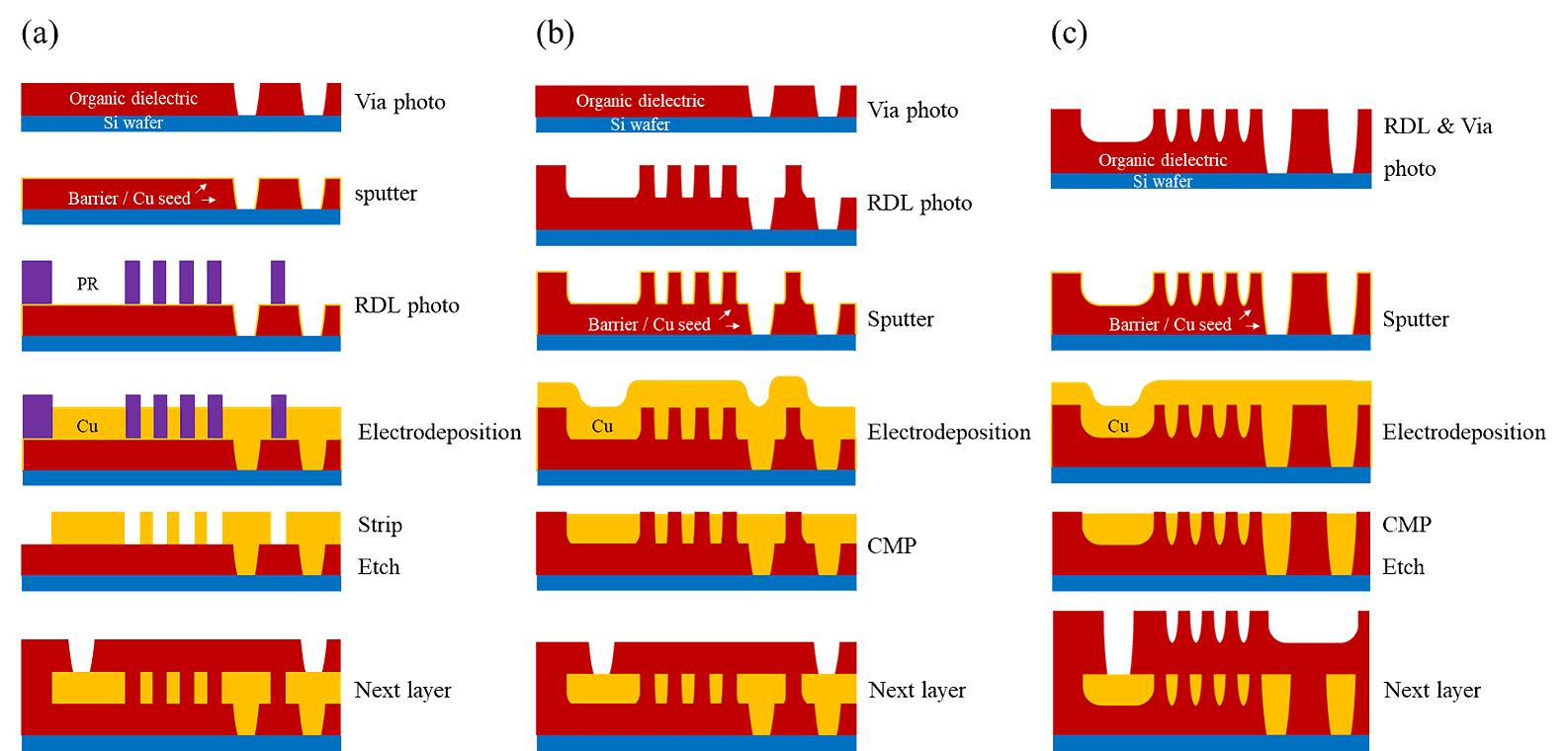
그림 2: (a) 반적층 프로세스(SAP), (b) 이중 다마신 공정, (c) 새로운 임베디드 트레이스 RDL 공정 순으로 이어지는 RDL 공정 흐름 개략도.
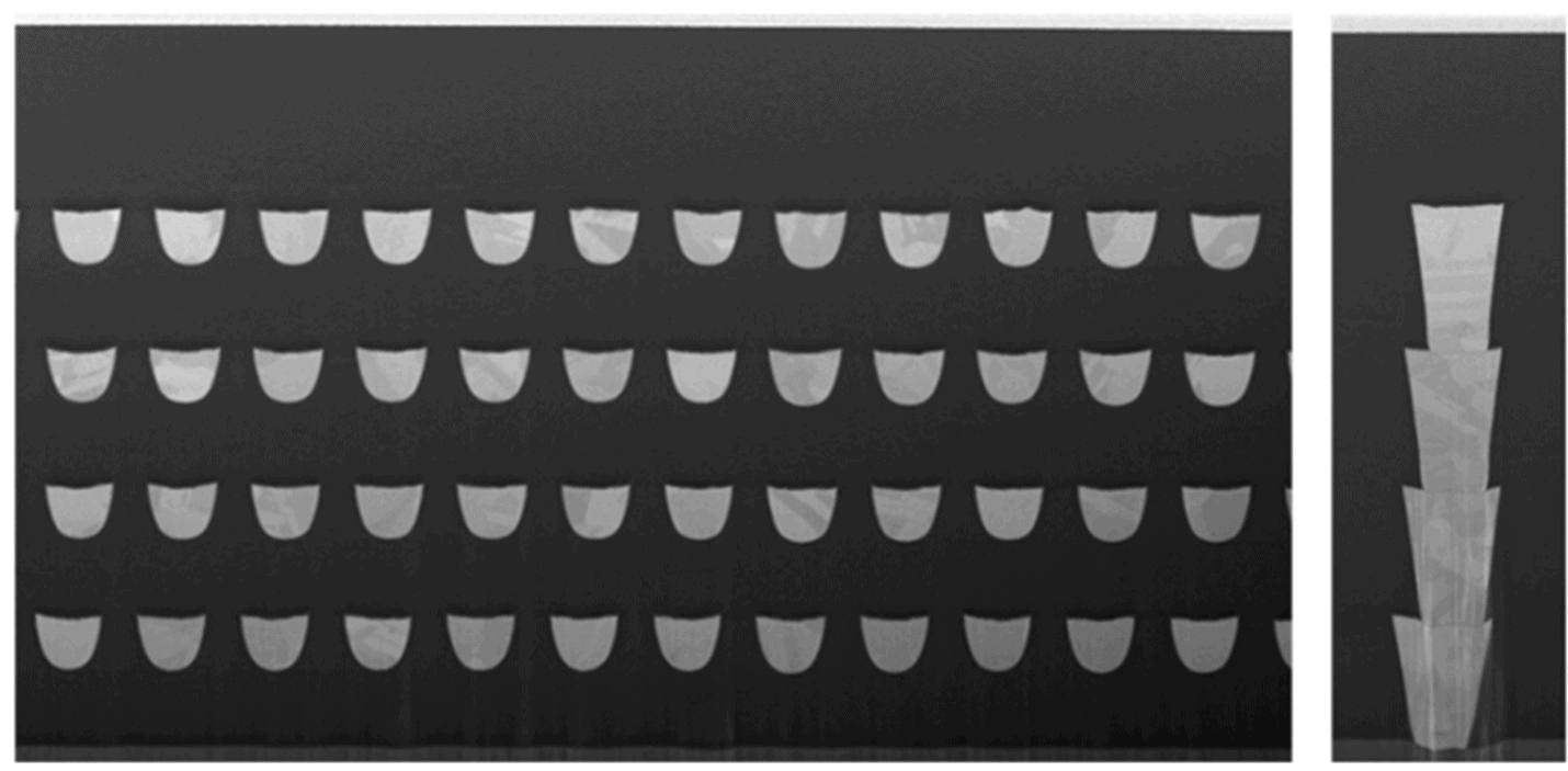
그림 3: ETR 공정을 통해 구현한 선폭/선간 2/1μm, 스택 비아 2μm의 4계층 RDL 단면도
안정성 및 성능
S-SWIFT 패키지의 ETR 구조는 철저한 테스트를 통해 신뢰성을 입증 받았습니다. ETR의 3개 면을 둘러싼 시드 층이 장벽 역할을 하여 전류, 열, 습도가 있는 환경에서 구리 이온 이동을 방지하고 신뢰성을 보장합니다. ETR을 장착한 S-SWIFT 패키지는 습기 흡수, 온도 순환, 불편 초가속 스트레스 시험, 고온 보관 시험 등 업계 표준 신뢰성 테스트를 통과했습니다.
결론
트레이스 RDL이 내장된 앰코테크놀로지의 S-SWIFT 패키징은 IC 패키징 기술의 비약적인 발전을 상징합니다. S-SWIFT는 기존 패키징 방식의 한계를 해결하고 안정적인 고성능 솔루션을 제공함으로써 AI, HPC, 데이터 센터 애플리케이션 수요 증가에 부응할 채비를 하였습니다. 업계가 계속해서 실리콘 기술의 한계를 극복함에 따라, S-SWIFT 같은 혁신은 고성능 컴퓨팅의 미래를 형성하는 데 중요한 역할을 할 것입니다. 자세한 내용은 Amkor.com/s-swift에서 확인하세요.
관련 게시물
Amkor Technology Receives Kioxia’s Best Partner Award

Amkor Earns Environmental Leadership Recognition from CDP
