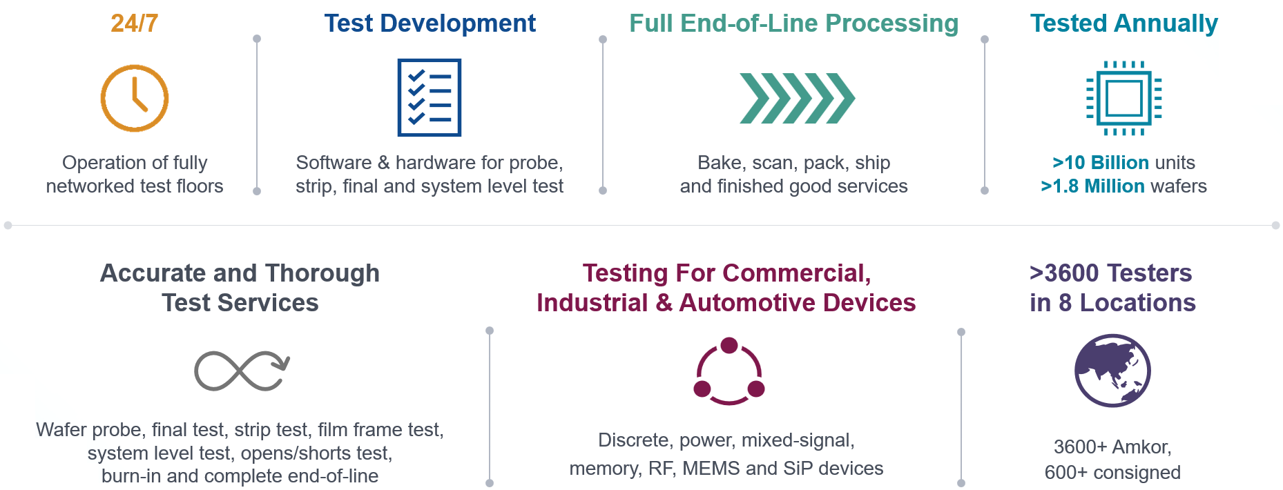
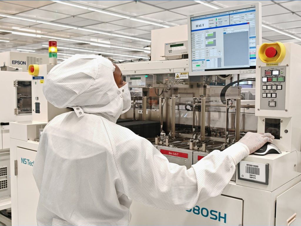
Innovative test solutions for diverse semiconductor system applications
With knowledge gathered from decades of supporting Tier 1 leaders and emerging industries, Amkor understands that test solutions must address advanced technology, quality, performance and cost of test. Through early engagement in each customer’s product lifecycle, Amkor helps define test strategies and intelligent equipment selection to provide differentiated test solutions.
Amkor offers comprehensive test services, including and not limited to, wafer level and package assembly. Amkor is the leading RF test services supplier engaged in ongoing joint efforts with test equipment suppliers and customers to enable 5G product production testing. As the top OSAT supplier for high performance compute (HPC), artificial intelligence (AI) processors & automotive testing, we have an extensive array of test capabilities and significant experience in device testing. The performance envelope for burn-in and system level test has recently expanded to account for higher power and lower cost.
テストシステム
Amkorは幅広い装置ラインアップを備え、また最新のデバイスをテストするために必要な最新設備を継続的に導入しています。
Application
- High performance compute, AI, power, memory, analog, RF, MEMS, sensor and SiP
テスター
- Clock: PEC clock rate, differential clocks, low Jitter, levels
- I/O: At-speed functional test. Low- & high-speed data I/O differential buses. Peripheral Event Controller (PEC) channel count, levels, timing – low EPA, patterns, test & measurements
- Power Delivery: Device power supply – channel count, levels, ganging, source and measure, high accuracy
- RF & Analog I/O: RF source & measure FE with optimal Rx/Tx port count to allow max parallelism for max UPH; ADC/DAC – resolution, accuracy, dynamic range to enable testing the latest technologies
- 最大UPH向けの最適な同時測定
ボード搭載
- PCB material, PCB width, trace impedance
- Per pin current capability, pin-to-pin crosstalk
- ツール向けRFIDモニタリング
- 温度許容差
Test Socket
- Per pin current capability, Pin count per DUT, Pin field planarity
- ピン to ピン・クロストーク/分離/シールディング
- 温度許容差
ハンドラ
- 自動温度制御/サーマルソーク
- DUTローテーション
- Footprint, loading force, loader speed
- Package handling, Position XY accuracy
Application
- Die sales – Low-power apps
- Chiplets – 2.5D, 3D – μbumps, hybrid bonding
- シリコンフォトニクス
テスター
- 高速ロジック、ミックスドシグナル、アナログ、高電力およびRF
- プローブピンのデータレート、電流密度、同時測定
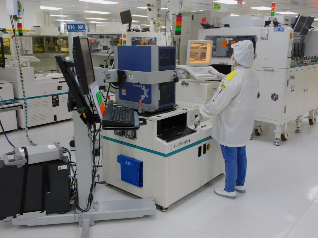
プローバ
- Wafer Size – 8” and 12” with 7, 5, 3, 2 nm process technologies
- Chuck planarity, Loading force, Position XY accuracy, Rotational angle
- Temperature Range
- Reconstituted wafers
プローブカード
- All docking types e.g., cable, pogo tower, direct dock
- In-line LASER cleaning, overdrive
- Probe card technologies: Cantilever, vertical, pogo, membrane, MEMS & dual-level Chip on Wafer (CoW)
- タッチダウン回数
- Pin count per DUT, pin-to-pin crosstalk, per pin current capability
- Pin field planarity, Alignment accuracy
Temperature tolerance
Application
- Logic, memory, automotive
- Sub 30W, Up to 200W, Up to 1000W
- Wafer level & package level
- Massively parallel test insertion
バーンイン・テスター
- 幅広いゾーン/チャンバー数
- 最大クロックレート
- 最大 I/O チャネル数
- 最大スロット数
- 製品認定および100%バーンイン対応
- 幅広いパワーレンジ
バーンインボード
- DUT power delivery: All power application ICs supported
- I/O およびクロックレートに対応
- ピンtoピン・クロストーク:ほぼすべてのアプリケーションで最小化
- ソケットの構成および機能
- ピンの最少化とバイアシングによるソケットコスト削減
- 高温の許容差
バーンイン・ハンドラー
- バーンイン・ボード(BIB)ローダー/アンローダー
バーンイン・ローダー/アンローダー(BLU)
- All popular package types are supported
- 高効率の入/出力
- Manual component & BIB loading/unloading: Discouraged for higher volumes & 100% burn-in, in the interest of efficient cycle times
Application
- High performance compute, Automotive, SiP
- Massively parallel test insertion
システムレベル・テスター
- Clock Rate: High
- I/O: Max slot count, max I/O channel count
- Power Delivery: Range ultra-low, low, medium, high, rail count
- 時間単位の最大ユニット
システムレベルテスト向けボード
- DUT power delivery – all power application ICs
- supported
- I/O およびクロックレートに対応
- Pin-to-pin crosstalk – minimal for most, if not all, applications
- ソケット構成および機能
- ピンの最少化とバイアシングによるソケットコスト削減
- 高温の許容差
システムレベル・ハンドラー
- 高テストパターンゾーン数
- 製品の認定および100%対応
- システムレベルロード/アンローダー
- All popular package types are supported
- High-efficiency I/O
- 温度制御器 - 低温ソークのオーバーヘッド時間
カスタマイズ可能なバックエンドプロセス
- ポストマーキングはオプション、ベークは耐湿レベル(MSL)に基づいて定められます
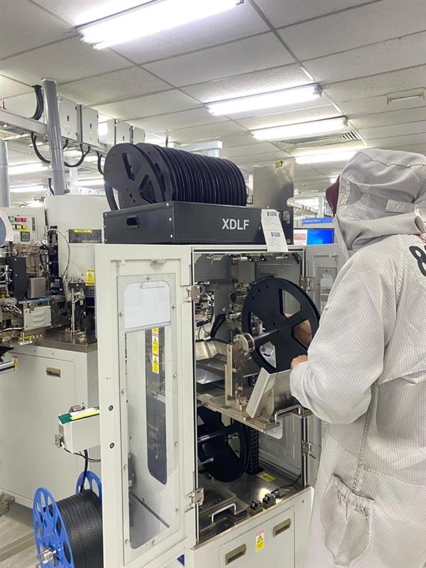
- 小型タレットハンドラーパッケージについては、ファイナルテスト、スキャンおよびテープ&リール梱包が一体機により連続的に行われます
高度な梱包のための高度なソリューション
- Package-on-Package (PoP)
- Through Silicon Vias (TSV)
- Flip Chip CSP (fcCSP)
- Flip Chip BGA (FCBGA)

テストロケーション
Our sites are strategically located near leading foundries, and major customer sites and co-located to support probe and test with assembly
Amkor Technology China (ATC) is located in the Pilot Free Trade Zone, which is only about 30 kilometers from two primary airports in Shanghai. The Free Trade Zone’s convenient logistics and business-friendly policies allow Amkor customers to deliver goods around the globe through value-added taxes or tax exemptions. ATC has 170,000 square meters of manufacturing space.
提供サービス
- ウェハプローブ
- フィルムフレームテスト
- パッケージテスト
- Burn-in test
- システムレベルテスト
- テスト開発
Packages
- CSP
- FCBGA
- フリップチップ
- MLF®/QFN
- PBGA
- WLCSP
マーケット
- 自動車向け
- コミュニケーション
- 民生品
- 産業向け
 Burn In
 Final Test
 End of Line (EOL)
 Memory Test Cell
 ATC1 – Shanghai
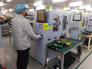
Amkor Technology Japan (ATJ) has seven factories and a head office. The head office is in Tokyo, which is only around 16 kilometers from HND airport and 5 kilometers from Tokyo Station. The factories are located all over Japan and the diversified manufacturing footprint is a key differentiator/competitive advantage that allows customers options to de-risk supply chains. ATJ has test experience with various semiconductor devices, e.g., Mix analog, Power discrete and module, System LSI and CIS and has 170,000 square meters of manufacturing space.
提供サービス
- ウェハプローブ
- パッケージテスト
- テスト開発
Packages
- Flip chip
- PBGA
- QFN
マーケット
- 自動車向け
- コミュニケーション
- メモリ
 Burn-in Test Cell
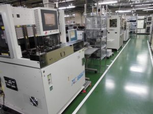 CCD Test Cell
 Memory Test Cell
 Final Test Cell
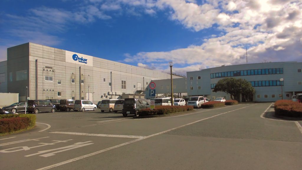 ATJ3 – Kumamoto
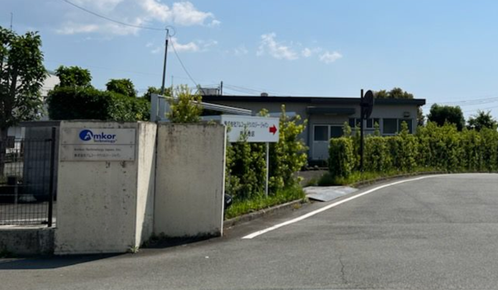 ATJ3 – Shisui
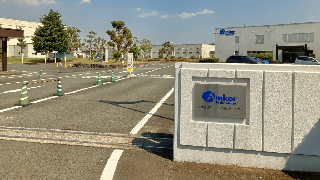 ATJ4 – Fukuoka
 ATJ4 – Kitakami
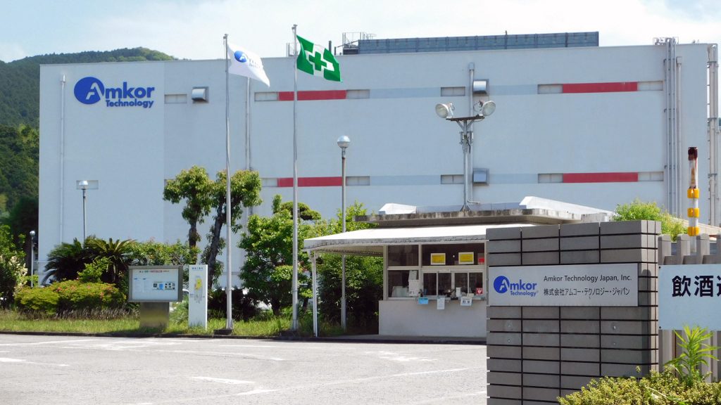 ATJ5 – Usuki
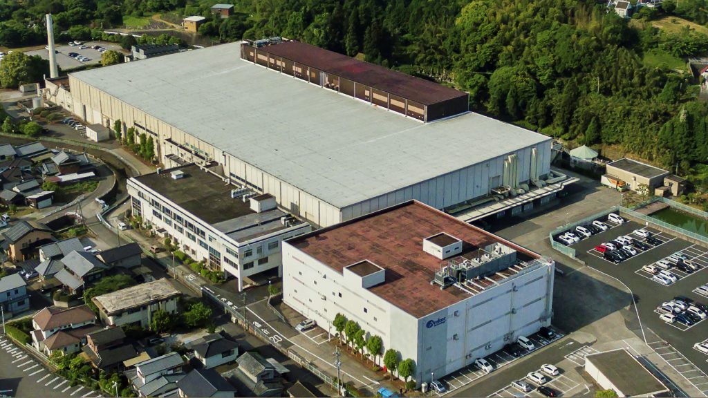 ATJ5 – Oita
 ATJ6 – Fukui
 ATJ7 – Hakodate
Amkor Technology Korea (ATK) operations encompass more than 11M ft2 of floor space with production facilities, product development centers, and sales and support offices strategically located in key electronics manufacturing regions. Our customers benefit from our extensive global footprint, enabling us to easily handle large orders and offer quick turnaround times. Our diverse portfolio includes stacked die, wafer level, MEMS, flip chip, Through Silicon Via (TSV) and 2.5/3D packaging, allowing us to be a single source for many customers. The ATK5 & ATK3 are about 34 kilometers away from Incheon airport. ATK4 is in the south of SKorea 335 kilometers from the Incheon airport.
提供サービス
- ウェハプローブ
- パッケージテスト
- フィルムフレームテスト
- システムレベルテスト
- テスト開発
- バンピング
Packages
- FCBGA
- fcCSP
- MLF®
- TQFP
- TMV®
- TSV – 2.5D, 3D
- WLCSP
マーケット
- High-Performance Compute (HPC)
- Artificial Intelligence (AI)
- 自動車向け
- コミュニケーション
- 民生品
 Pick & Place Handler
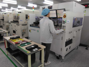 Pick & Place Handler
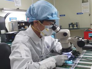 Test Hardware Repair Station
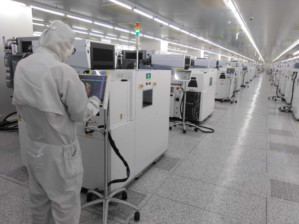 Final Test Lot Introduction
 ATK3 – Incheon
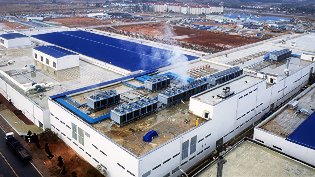 ATK4 – Gwangju
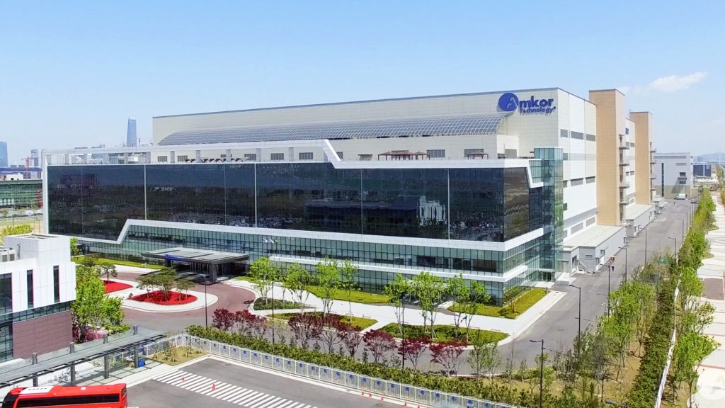 ATK5 – Incheon
Amkor Technology Malaysia (ATM) is located in Malaysia’s Free Industrial Zone, about 50 kilometers from Kuala Lumpur city center and Kuala Lumpur International Airport. The Free Trade Zone’s convenient logistics and business-friendly policies allow Amkor customers to deliver goods around the globe through value-added taxes or tax exemptions. ATM has 32,000 square meters of manufacturing space and 108,800 square meters of land.
提供サービス
- パッケージテスト
Packages
- SO8-FL
- SONXXX-FL
- TO-220FP
- TQFP
- TSON-FL
マーケット
- ディスクリート
- Power
 End of Line (EOL)
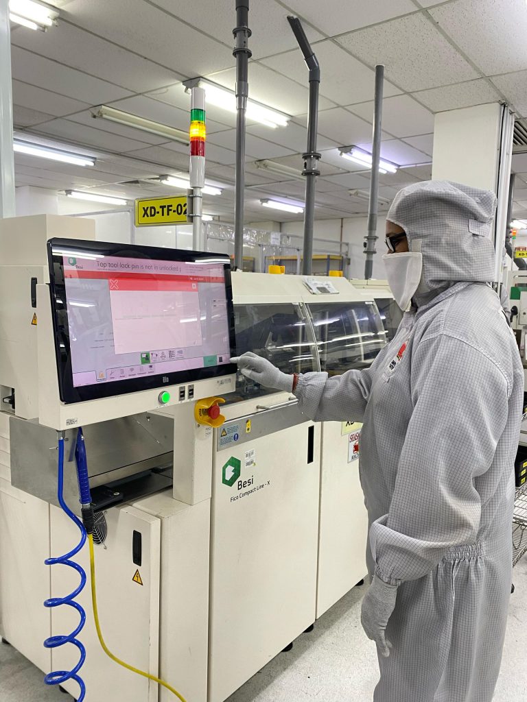 SO8 Package Final Test
 ATM1 – Malaysia
Amkor Technology Philippines (ATP) provides a full range of assembly and test services. ATP has two factories located in Muntinlupa City (P1) and Binan City, Laguna (P3/P4) to serve our global clientele. ATP P1, Muntinlupa City – has a manufacturing space of 32,000 sqm that is dedicated to producing legacy lead frame products.
ATP P3/P4, Binan City, Laguna, with a size of 32,800 sqm, is leading the way in advanced packaging technologies. P3 Assembly is recognized for its advanced packages and serves as a manufacturing and development center for MEMS and sensors. Amkor’s testing facility in P4 has been offering wafer probe and final testing services for the past 30 years, managing a wide range of applications including power and microcontrollers to MEMS.
With ATP registered with the Philippines Economic Zone Authority (PEZA), Amkor customers can enjoy significant benefits. The benefits consist of shipping products worldwide with incentives, VAT zero rating, and preferential tax rates, which guarantee a cost-efficient and efficient supply chain.
ATP has earned a reputation for its reliable packaging technology innovations and testing facilities. Our operational base encompasses both production and product development, which enables us to meet the changing demands of the semiconductor industry.
提供サービス
- ウェハプローブ
- パッケージテスト
- フィルムフレームテスト
- システムレベルテスト
- テスト開発
- MEMS Test
- バーンイン
Packages
- MLF®
- リードフレーム
- QFP
マーケット
- 自動車向け
- 民生品
- メモリ
 ウェハプローブ
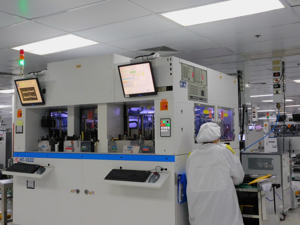 Final Test Pick & Place Handler
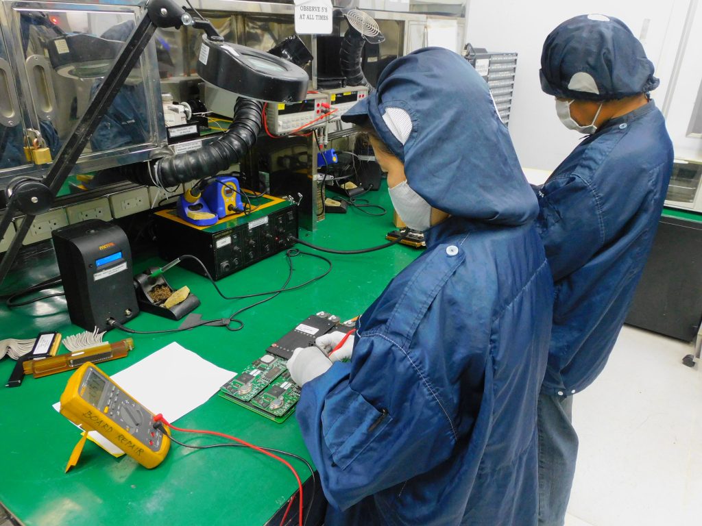 Test Hardware Repair Station
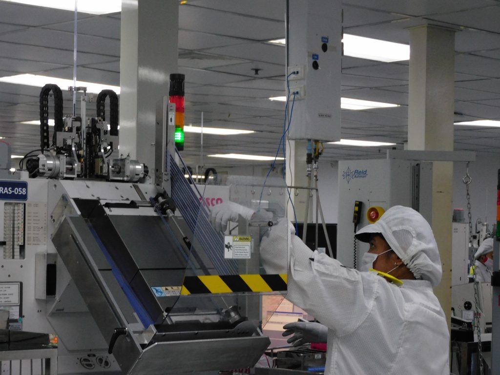 Final Test Gravity Feed Handler
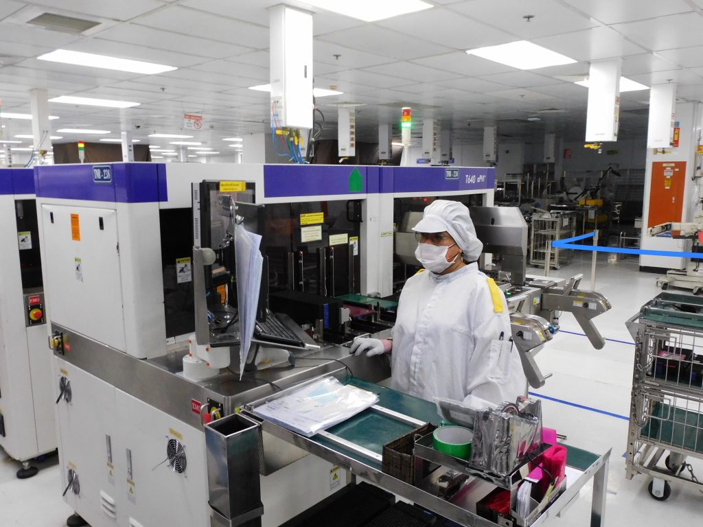 Post Test Tape & Reel Handler
 Burn-in Manual Load & Unload
 ATP3 – Philippines
Amkor Technology Portugal (ATEP) is located near Porto, the second biggest city in Portugal and fifteen minutes away from the international airport and seaport with excellent direct connections inside Europe and to the rest of the World. Being the biggest Outsourced Semiconductor Assembly and Test facility in Europe, dedicated to Advanced Packaging, the location benefits from accumulated Semiconductor Assembly and Test experience in the region for more than five decades. ATEP currently has 20,000 square meters of clean room space and is expanding to 50,000 square meters.
提供サービス
- ウェハプローブ
- テスト開発
Packages
- FCBGA
- WLCSP
- WLFO
マーケット
- 自動車向け
- コミュニケーション
- メモリ
 Opens & Shorts Test Handler
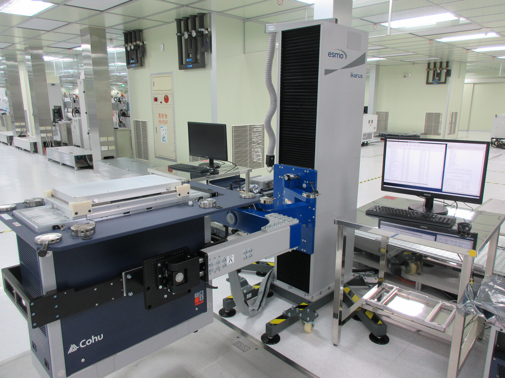
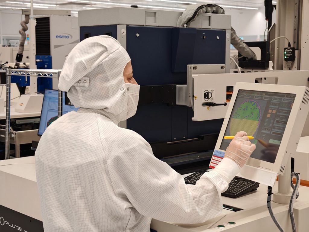 Cohu Tester
 Test Hardware Storage System
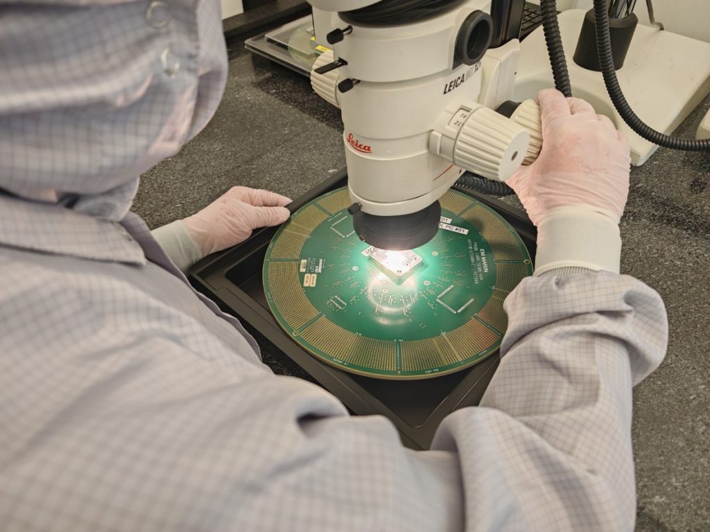 Test Hardware Repair Station
 V93000 Wafer Probe Test Cell
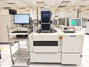 Cohu/Semics Wafer Probe Test Cell
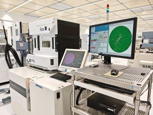 Ultraflex Wafer Probe Test Cell
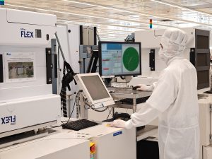 Ultraflex Wafer Probe Test Cell
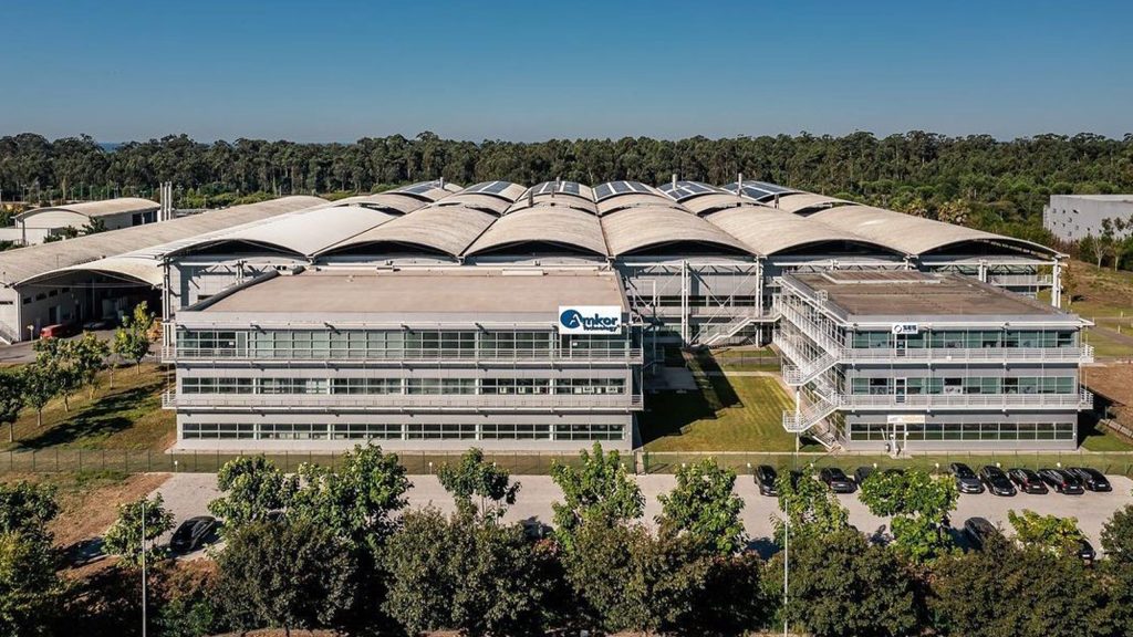 ATEP – Portugal
Amkor Technology Taiwan (ATT) is situated in the HsinChu scientific area’s Taiwan Semiconductor Circle ecology, and it takes 30 minutes to reach the airport and wafer foundries. With Full-TurnKey solution services that include Bump/CP/WLCSP & Bump/CP/FCBGA/FT, Amkor Technology Taiwan (ATT) focuses on advanced packages (Bump, WLCSP and FCBGA). Additionally, ATT provides RD resources to help clients with complete solution design, including package, test program, and assembly development. ATT has 48,000 square meters of cleanroom manufacturing space.
提供サービス
- ウェハプローブ
- パッケージテスト
- フィルムフレームテスト
- バンピング
Packages
- Bumped wafer
- WLCSP
- fcCSP
- FCBGA
- SiP
マーケット
- コミュニケーション
- 民生品
- ネットワーク
 Final Test Tester
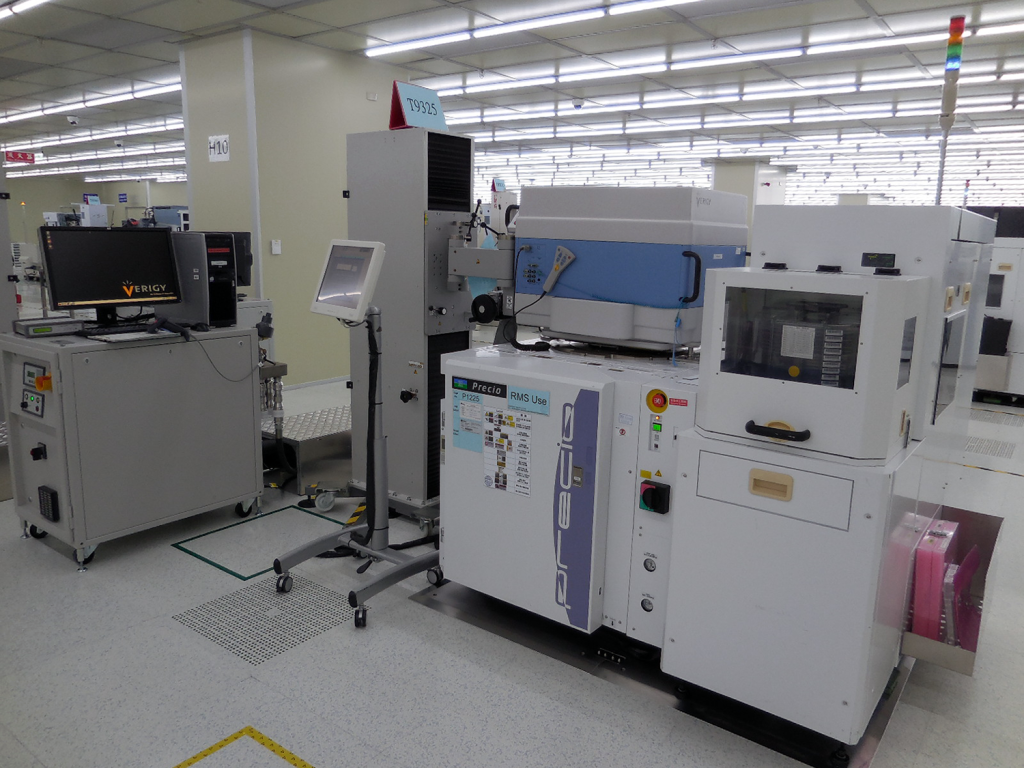 Wafer Probe Test Cell
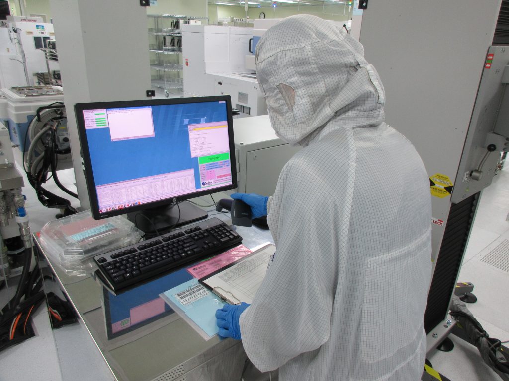 Operator Performing Lot Introduction
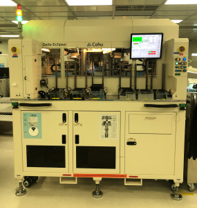 Final Test Handler
 ATT1 – Taoyuan City
 ATT3 – Hukou Township
 ATT6 – Taoyuan City
Amkor Technology Vietnam (ATV) is situated in Bac Ninh, and it takes 25 minutes to reach the airport. This site provides System-In-Package and Memory package and test services. Additionally, ATV provides RD resources to help clients with complete solution design, including package, test program, and assembly development. ATV has a large area of cleanroom manufacturing space.
提供サービス
- ファイナルテスト
- システムレベルテスト
- テスト開発
Packages
- SIP – SoC, SoC
+ Memory PoP, double sided stacked - メモリ
- AiP, AoP
マーケット
- コミュニケーション
- 民生品
 SLT
SLT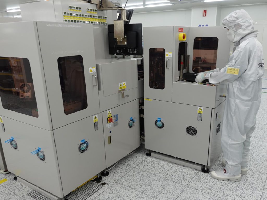 SCAN
SCAN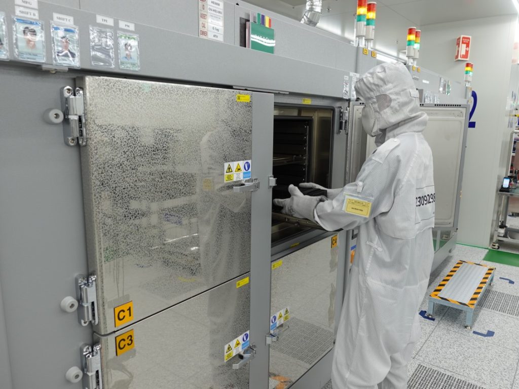 Bake
Bake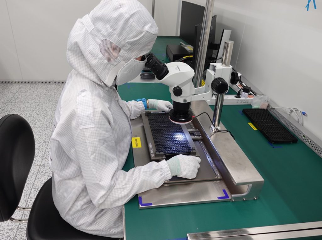 FVI Check
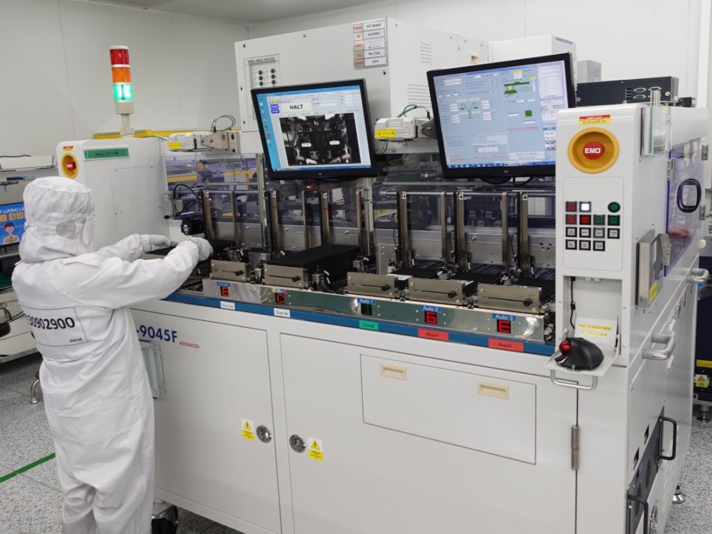 Cohu Final Test with Pick & Place Handler
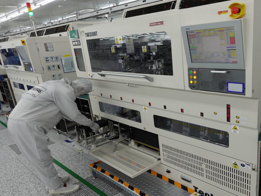 TekWing Memory Test
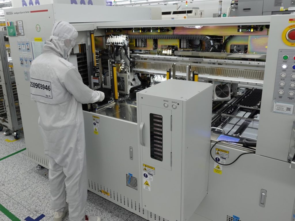 Memory Test Cell
 Test Hardware Repair Station
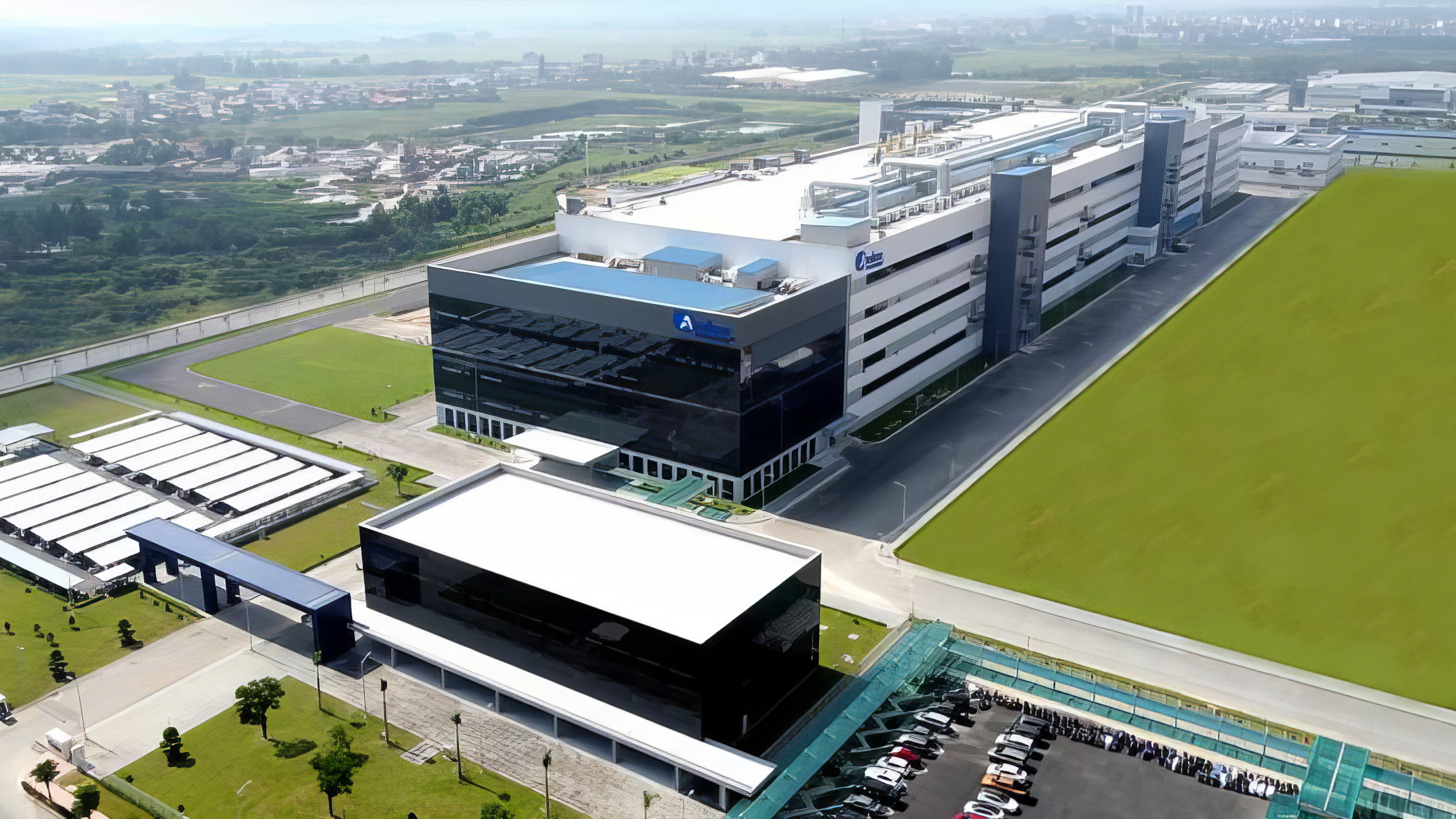 ATV – Vietnam
テスト開発エンジニアリング
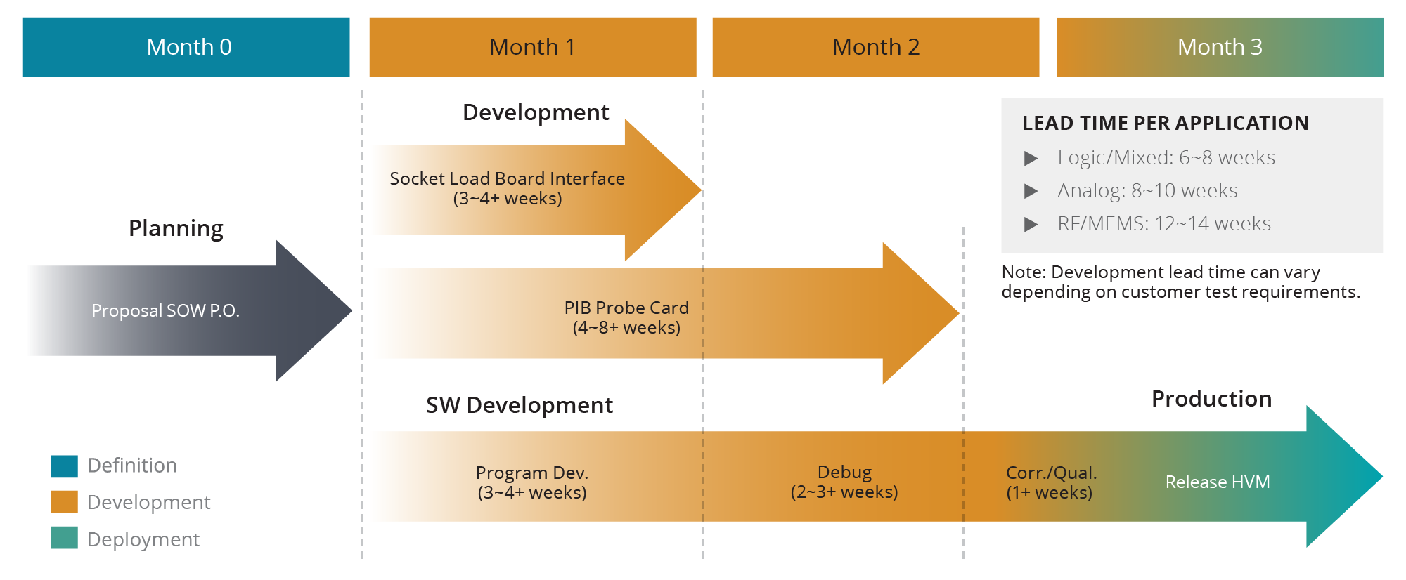
お客様は自社でテストソリューションを開発し、量産時にAmkorへ委託することが可能です。またAmkorは、ソフトウェアとハードウェアのソリューションの共同開発や、すべてのテスト開発を受託することも可能です。最大限のパフォーマンスを発揮するためには製品設計の早期のタイミングから当社と連携頂くことがベストですが、製品ライフサイクルの後半でコスト効率の高いテスターおよび(または)高度な多数個同時測定への移行を行うことでも大幅なコストダウンを提供いたします。
一般的なテスト開発のサイクルタイム
市場別の差別化されたテスティング
Amkor is the number one automotive OSAT, supporting worldwide supply chains. Products in this area include infotainment and safety (ADAS) requiring high levels of performance. This requires a comprehensive set of test during the production test workflow.
- Cold wafer probe, room & hot temperature final test
- 高品質で規格に準拠したプロセスおよびシステム
- Inspections and multi-temperature test capabilities
- ウェハプローブ:-55°C~+200°C
- -55°C ~ +175°Cでのファイナルテスト
- バーンイン
- システムレベルテスト(SLT)
- 低温ウェハプローブを活用することで、ファイナルテストは室温と高温のみのテストを行います
- Post-assembly opens/shorts testing includes 2 and 4-wire resistance tests
The largest fraction of Amkor’s revenue is derived from the Communications market segment. This includes smartphones, tablets, handhelds and wearable devices. Our leading-edge test solutions keep pace with rapid changes in cellular and connectivity technology requirements. Amkor is well-positioned for 5G RF wireless products and their test requirements.
- RF 5G NR Conductive test for both FR1 and FR2 frequency ranges
- Asynchronous test for a multitude of RF connectivity standards
- 32ポート、マルチサイト、マルチチャネル Tx/Rx対応ATE
- RF コールボックステスト含むシンプルなSLTを使用し複雑なSiPに対応
- ローカルRFシールディング ≤60 dBm
- コストを低減するマルチサイトx8 RFテスト
- RFフロントエンド(RFFE)、SiPおよび IoT
- WLCSP向けKnown Goood Die(KGD)、SiP向けKnown Tested Die(KTD)のRFウェハプローブ対応
- 単一および複数チャネルのビームフォーミング、位相配列、AiP/AoP対応
- SoC + メモリ PoPーダブルサイドテスト/スタック CSP - メモリおよびロジックテスト
Amkor is a leading provider of high-performance test solutions for the demanding networking and high-performance compute market. This market segment is driving the need for multiple chiplets that include artificial intelligence (AI) accelerators, central processing units (CPU), graphics processing units (GPU), field-programmable gate array (FPGA), input/output (I/O), serializer/deserializer (SERDES – PCIe, CXL), silicon (Si) photonics. Integral to these markets are advanced memory technologies like high bandwidth memory (HBM) and migrations from hard disk drives to solid-state drives (SSD), with NAND memories.
- Distributed test (wafer probe, in-situ test between key assembly steps and final test (SLT and ATE) for 2.5D & 3D). Probe solutions and wafer map management for chip-on-wafer (CoW)
- Active thermal control (ATC) for up to 300-watt & up to 1000W products across tri-temperature in SLT and ATE test
- Dynamic burn-in. Test during burn-in (TDBI)
- フィルムフレームおよびストリップテスト(x308 EEPROM)
- 最大 16 Gbps および 32 Gbpsまでの高速シリアルデジタルの検査(例:PCIe、第4世代、第5世代)
- シリコンフォトニクスIC
Amkor is a leader in power discrete devices & modules like Diodes, Flip chip MOSFETs, Intelligent power modules, Insulated-Gate Bipolar Transistors (IGBT), Multi-voltage FETs, Regulators and bipolar transistors for the automotive, power transmission and industrial segments. Amkor’s test services are closely integrated with the assembly flow for shorter cycle times and reduced costs. Key characteristics include:
- 高電流、高電圧
- ケルビンコンタクトタイプテスト
- 低 Rds_on
- Si, SiC, Gan
Products for today’s Internet of Things (IoT) and Industrial Internet of Things (IIoT) require an MCU, RF transmitter/receiver, sensors and actuators. Sensor technologies include and are not limited to magnetometers, accelerometers, gyroscopes, proximity, RF switches, photo sensors, microphones, micro-speakers, humidity, pressure, and temperature. The test solution needs to cover the conversion of these physical real-world analog signals in a variety of range of operations into an electrical stimulus that is tested during the production workflow.
ご質問やお問合せはこちらまで
以下の「リクエスト」をクリックしてご連絡ください