
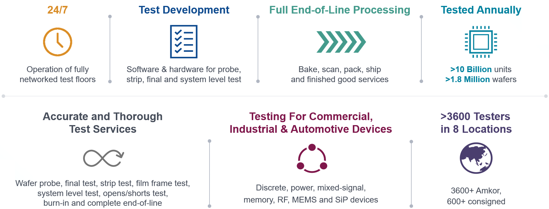
多様な半導体システムアプリケーション向けの革新的なテストソリューション
数十年におよぶTier 1のお客様や業界のリーディングカンパニーとのビジネスで培った知見から、当社はテストソリューションとは高度な技術、品質、性能をリーズナブルなコストで提案しなければいけないという事を熟知しています。お客様の製品ライフサイクルに早期から関わることで、テスト戦略および的確な設備選定をサポートし、最適化されたテストソリューションを提供します。
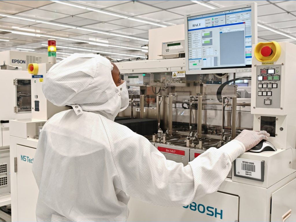
Amkorは、ウェーハレベルおよびパッケージ組立を含む(これらに限定されない)包括的なテストサービスを提供しています。さらに、テスト装置サプライヤーおよびお客様との継続的な共同努力を通じて、5G製品の量産テストを可能にする業界をリードするRFテストサービスプロバイダーです。ハイパフォーマンスコンピューティング(HPC)、人工知能(AI)プロセッサ、自動車向けテストにおけるトップOSATサプライヤーとして、当社は広範なテスト機能と豊富なデバイステストの実績があります。最近では、バーンインおよびシステムレベルテストの性能範囲が拡大し、高電力および低コストに対応可能となりました。
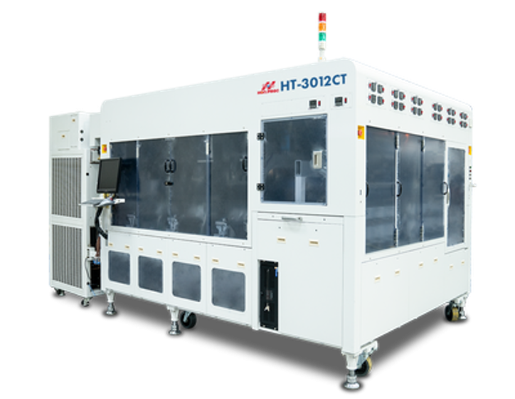
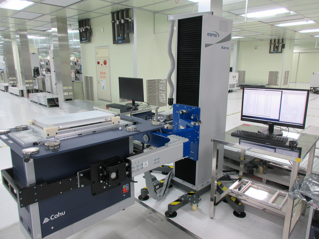
テストシステム
Amkorは幅広い装置ラインアップを備え、また最新のデバイスをテストするために必要な最新設備を継続的に導入しています。
アプリケーション
- ハイパフォーマンスコンピューティング(HPC)、AI、パワー、メモリ、アナログ、RF、MEMS、センサー、SiP
テスター
- クロック:PECクロックレート、差動クロック、低ジッター、レベル制御
- I/O:アットスピードのファンクショナルテスト、低速および高速のデータI/O差動バス、周辺イベントコントローラ(PEC)チャネル、レベル、タイミング - 低EPA、パターン、テストと測定
- 電力供給:デバイス電源 – チャネル数、レベル、ギャンギング、ソース測定、高精度
- RFとアナログ I/O デバイス:RFソースおよび最大UPH向けに最大同時測定を可能にするため最適なRx/Txポート数でFEを測定します、ADC/DAC - 最新の技術を提供するための解像度、精度、ダイナミックレンジ
- 最大UPH向けの最適な同時測定
ボード搭載
- PCB材料、PCB幅、配線インピーダンスなど、複数の設計・製造要素における高い性能
- ピン単位の電流対応能力、ピン間クロストーク
- ツール向けRFIDモニタリング
- 温度許容差
テストソケット
- ピン単位の電流対応能力、DUTあたりのピン数、ピンフィールドの平坦性
- ピン to ピン・クロストーク/分離/シールディング
- 温度許容差
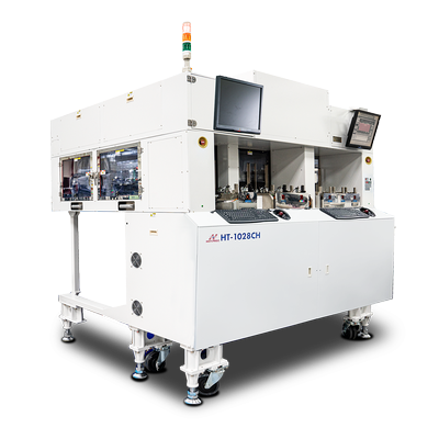
ハンドラ
- 自動温度制御(ATC)/サーマルソーク
- 最大3200W(リファレンスマシンでは最大5000W)までの高電力対応
- DUTローテーション
- フットプリント、接触力最大650 kg(RMでは最大980 kgの加圧力)、ローダー速度
- パッケージハンドリング、位置XY精度
アプリケーション
- ダイ販売 – 低消費電力アプリケーション向け
- チップレット – 2.5D、3D – マイクロバンプ、ハイブリッドボンディング
- シリコンフォトニクス
テスター
- 高速ロジック、ミックスドシグナル、アナログ、高電力およびRF
- プローブピンのデータレート、電流密度、同時測定
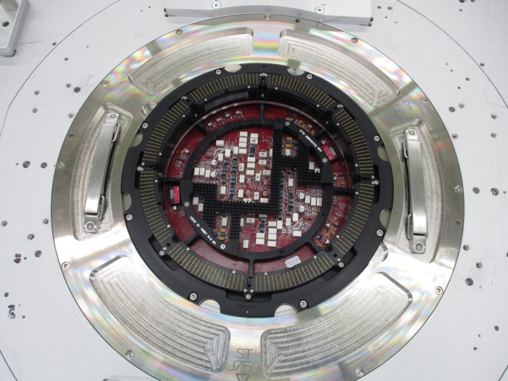
プローバ
- ウェーハサイズ:8インチおよび12インチ(7nm、5nm、3nm、2nmのプロセス技術に対応)
- チャックの平坦性、加圧力、XY位置精度、回転角度
- 温度範囲
- 再構成ウェーハ
プローブカード
- すべてのドッキングタイプ、例ケーブル、ポゴタワー、ダイレクトドック
- インラインレーザークリーニング、オーバードライブ
- プローブカード技術:カンチレバー型、垂直接続型、ポゴピン型、メンブレン型、MEMS型、およびデュアルレベルチップ・オン・ウェハ(CoW)
- タッチダウン回数
- DUP毎のピン数、ピン to ピン・クロストーク、ピン単位電流管理
- ピンフィールドの平坦性、アライメント精度
耐温度性
アプリケーション
- ロジック、メモリ、自動車向け
- サブ30W、最大200W、最大1000W
- ウェハーレベルおよびパッケージレベル
- 大規模並列テスト挿入
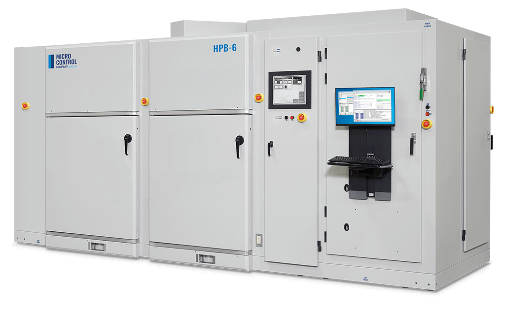
バーンイン・テスター
- 幅広いゾーン/チャンバー数
- 最大クロックレート
- 最大 I/O チャネル数
- 最大スロット数
- 製品認定および100%バーンイン対応
- 幅広いパワーレンジ
バーンインボード
- DUP電源供給:すべての電力アプリケーションICに対応
- I/O およびクロックレートに対応
- ピンtoピン・クロストーク:ほぼすべてのアプリケーションで最小化
- ソケットの構成および機能
- ピンの最少化とバイアシングによるソケットコスト削減
- 高温の許容差
バーンイン・ハンドラー
- バーンイン・ボード(BIB)ローダー/アンローダー
バーンイン・ローダー/アンローダー(BLU)
- すべての一般的なパッケージに対応
- 高効率の入/出力
- 手動コンポーネントおよびBIBローディング/アンローディング:効率的なサイクルタイムの観点から大量生産や100%バーンインには非推奨
アプリケーション
- ハイパフォーマンスコンピューティング(HPC)、自動車向け、SiP
- 大規模並列テスト挿入
システムレベル・テスター
- クロックレート:高
- I/O:最大スロット数、最大I/Oチャネル数
- 電力供給:超低電力から低・中・高電力までの幅広い範囲、レール数の対応
- 時間単位の最大ユニット
システムレベルテスト向けボード
- DUT電源供給—すべてのパワーアプリケーションIC
- に対応
- I/O およびクロックレートに対応
- ピン間クロストーク:ほとんどのアプリケーション、場合によってはすべてにおいて最小化
- ソケット構成および機能
- ピンの最少化とバイアシングによるソケットコスト削減
- 高温の許容差
システムレベル・ハンドラー
- 高テストパターンゾーン数
- 製品の認定および100%対応
- システムレベルロード/アンローダー
- すべての一般的なパッケージに対応
- 高効率 I/O
- 温度制御器 - 低温ソークのオーバーヘッド時間
カスタマイズ可能なバックエンドプロセス
- ポストマーキングはオプション、ベークは耐湿レベル(MSL)に基づいて定められます
- 小型タレットハンドラーパッケージについては、ファイナルテスト、スキャンおよびテープ&リール梱包は順次行われます
高度な梱包のための高度なソリューション
- Package-on-Package (PoP)
- シリコン貫通ビア(TSV)
- Flip Chip CSP (fcCSP)
- Flip Chip BGA(FCBGA)

テストロケーション
テスティングロケーションは主要なファンドリや主要なお客様のサイトに近接または共同敷地内に戦略的に配置され、プローブテストに対応しています。
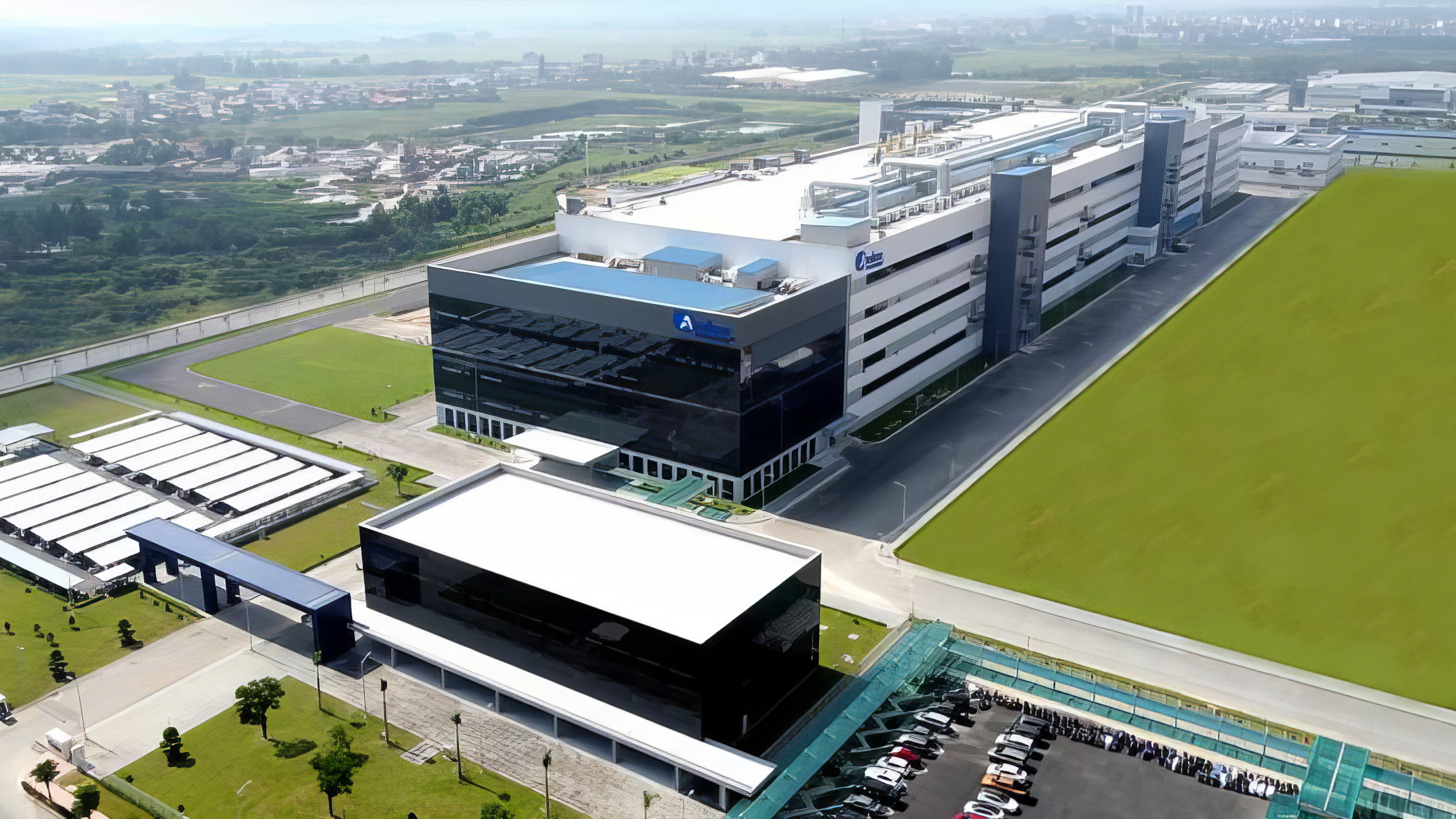
Amkor Technology Korea(ATK)は韓国全土に戦略的な製造施設を運営しており、11M平方フィート²を超える生産スペースを網羅しています。当社の施設には、主要なエレクトロニクス製造地域にサービスを提供する高度な製品開発センターと包括的な販売サポートオフィスが含まれています。
当社の多様な技術ポートフォリオには、スタックダイ、ウェーハレベル、MEMS、フリップチップ、シリコン貫通ビア(TSV)、および2.5D/3Dパッケージングソリューションが含まれており、複雑な半導体パッケージングニーズに対してワンストップで対応可能です。
仁川国際空港近郊に位置するATK5およびATK3施設、ならびに光州にあるATK4施設を活用し、世界中のお客様向けの短納期対応および大口受注のスムーズな処理を支える効率的なロジスティクス体制を構築しています。
提供サービス
- テスト開発
- ウェハプローブ
- パッケージテスト
- フィルムフレームテスト
- システムレベルテスト
- バンピング
Packages
- FCBGA
- fcCSP
- MLF®
- TQFP
- TMV®
- TSV – 2.5D、3D実装
- WLCSP
マーケット
- 高性能コンピューティング(HPC)
- AI(人工知能)
- 自動車向け
- コミュニケーション
- 民生品
自動化
- 自律移動式バスケット/ロボット
- ソケットクリーニング
- テストプログラム管理者
- 自動テストプログラムローディング
- 自動歩留まりモニター/データ分析/レポート
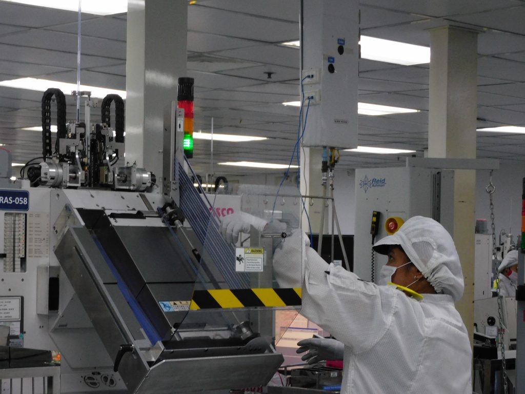
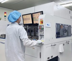 電気テスト
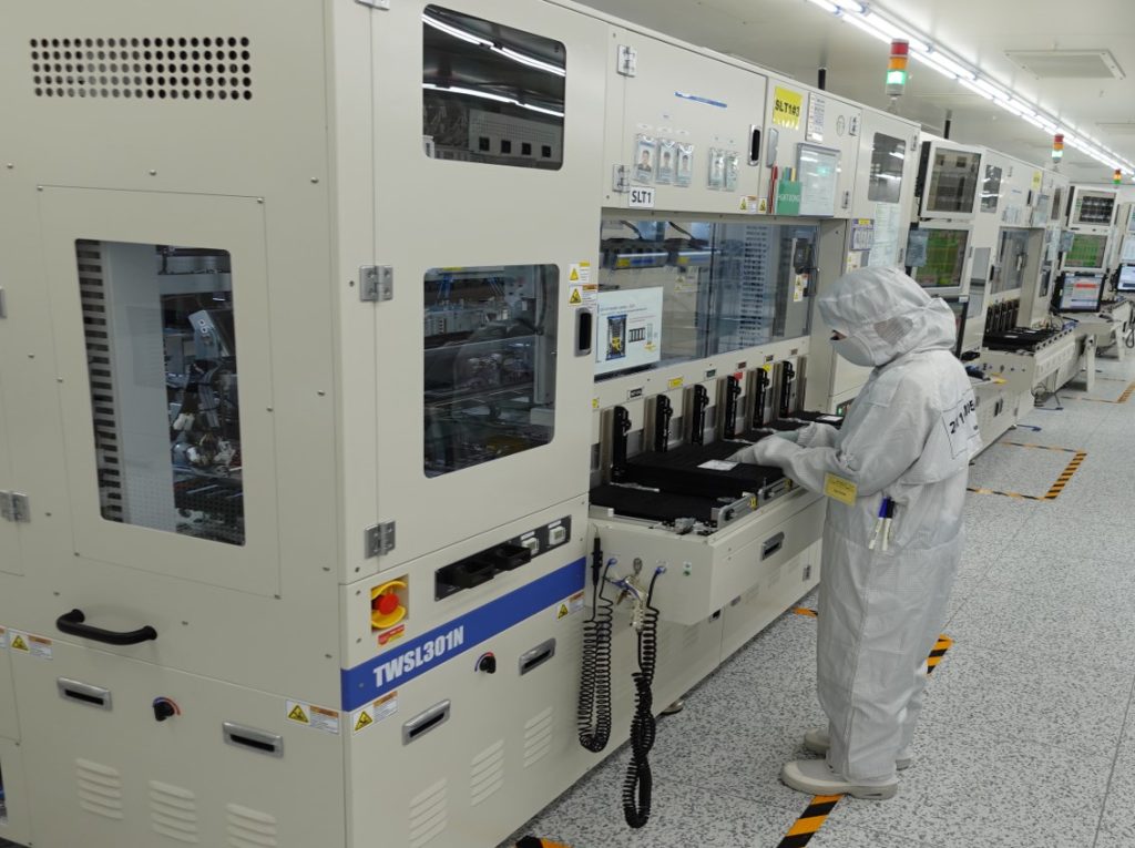
電気テスト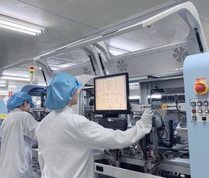 システムレベルテスト
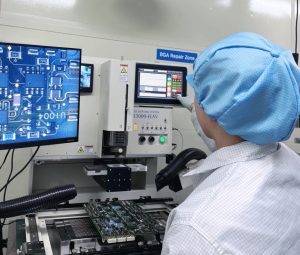 テストハードウェア修理ステー
ション
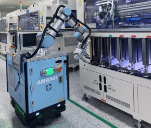 自律移動ロボット(Autonomous Mobile Robot)
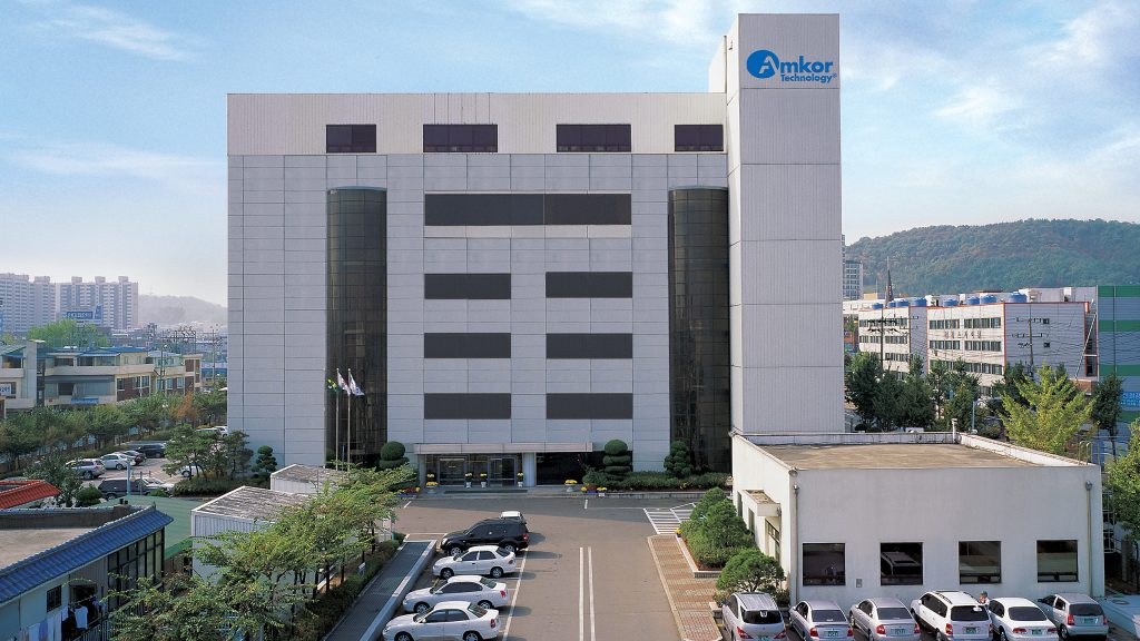 ATK3 – 仁川
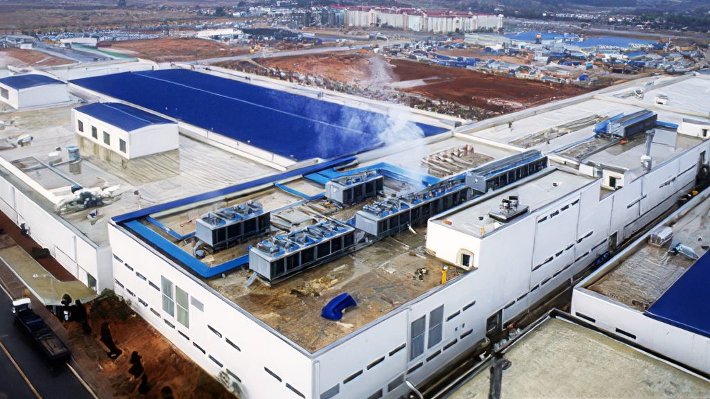 ATK4 – 光州
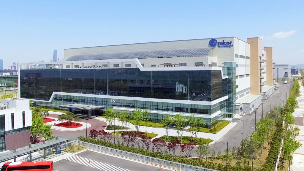 ATK5 – 仁川
Amkor Technology Taiwan(ATT)は、新竹サイエンスパーク内の台湾半導体エコシステムに位置しており、空港およびウェーハファウンドリへは30分でアクセス可能です。Bump/CP/WLCSPおよびBump/CP/FCBGA/FTを含むフルターンキーソリューションサービスを提供し、Bump、WLCSP、FCBGAなどの先端パッケージに注力しています。さらにATTでは、パッケージ設計、テストプログラム開発、実装開発を含む包括的なソリューション設計を支援するR&Dリソースも提供しています。クリーンルーム製造スペースは48,000平方メートルに及びます。
提供サービス
- ウェハプローブ
- パッケージテスト
- フィルムフレームテスト
- バンピング
Packages
- Bumped Wafer
- WLCSP
- fcCSP
- FCBGA
- SiP
マーケット
- コミュニケーション
- 民生品
- ネットワーク
 ファイナルテストテスター
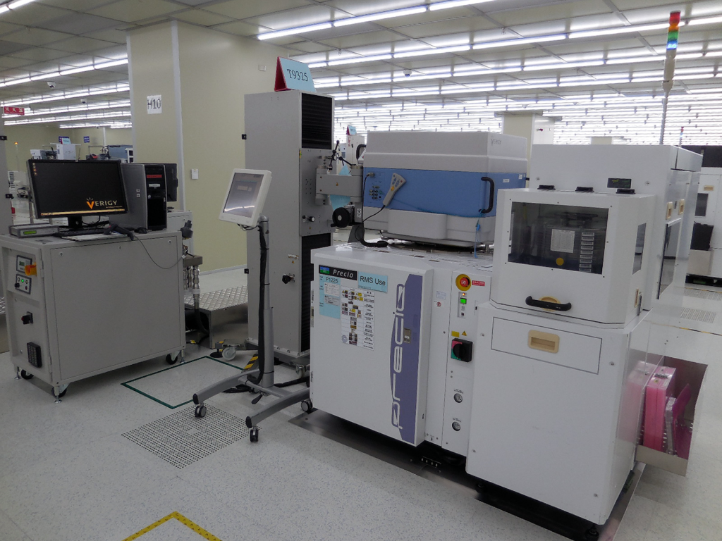 ウェーハプローブテストセル
 オペレーターによるロット導入作業
 最終テストハンドラ
 ATT1 – 桃園市
 ATT3 – 湖口商業地域
 ATT6 – 桃園市
Amkor Technology Japan(ATJ)は、7つの工場と本社を有しています。本社は東京にあり、羽田空港から約16キロメートル、東京駅から約5キロメートルという便利な立地にあります。工場は日本各地に分散しており、多様な製造拠点は、サプライチェーンのリスクを軽減するための選択肢をお客様に提供するという、ATJの大きな差別化要因かつ競争優位性となっています。ATJは、ミックスドアナログ、パワー離散・モジュール、システムLSI、CIS(CMOSイメージセンサ)など、さまざまな半導体デバイスのテスト実績があり、製造スペースは17万平方メートルに及びます。
提供サービス
- ウェハプローブ
- パッケージテスト
- テスト開発
Packages
- フリップチップ
- PBGA
- パワーディスクリート
- パワーモジュール
- QFN
マーケット
- 自動車向け
- コミュニケーション
- 民生品
- 産業向け
 バーンインテストセル
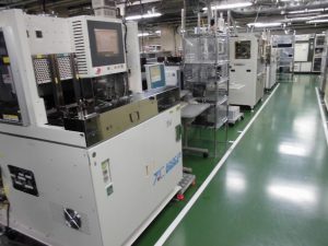 CCDテストセル
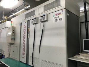 メモリテストセル
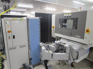 最終テストセル
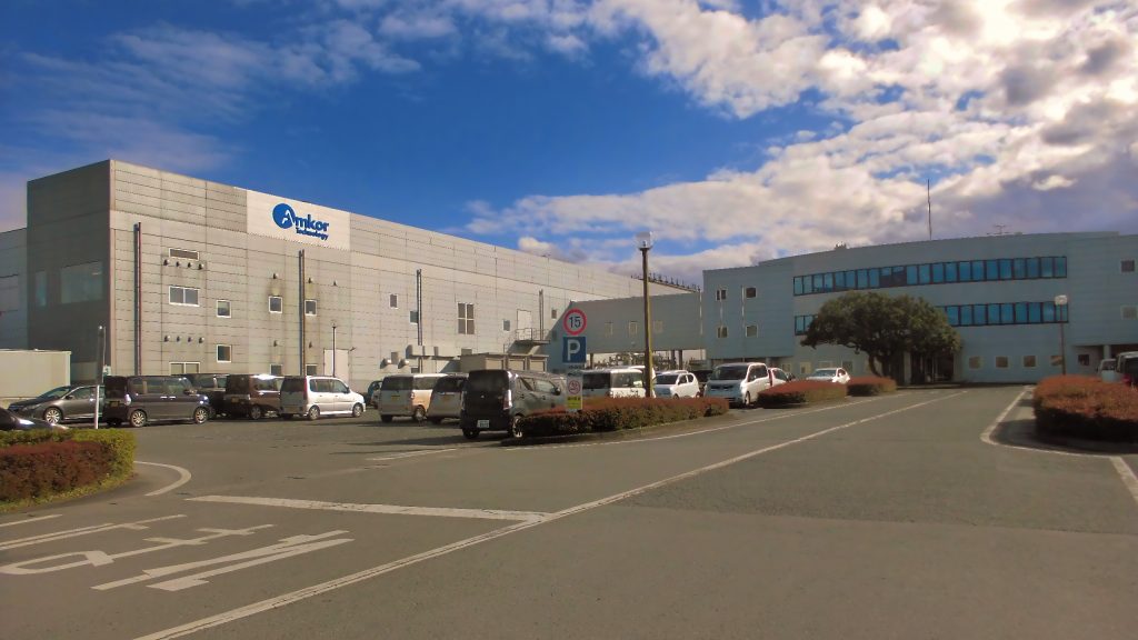 ATJ3 – 熊本
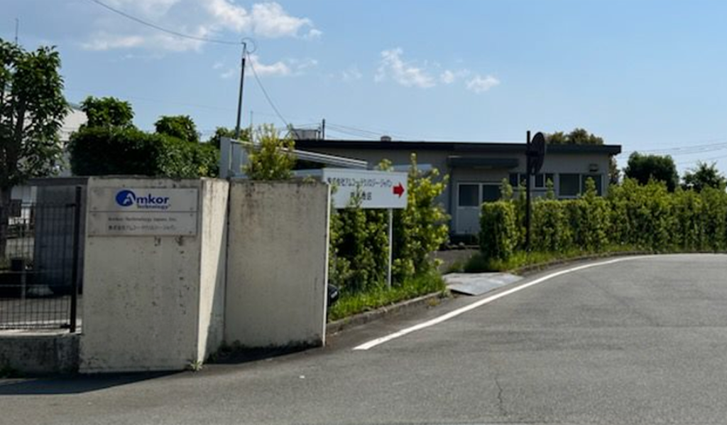 ATJ3 – 泗水
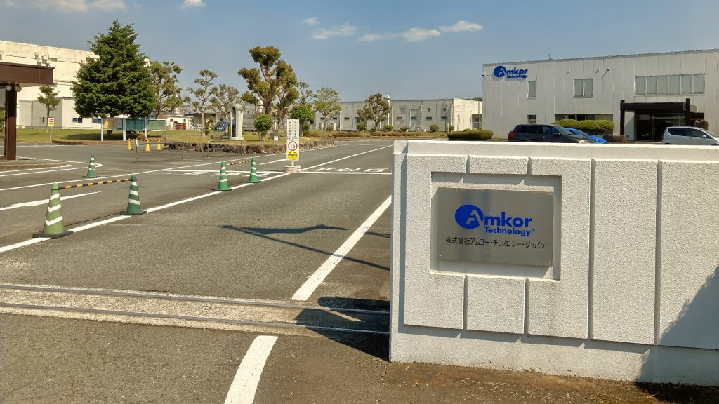 ATJ4 – 福岡
 ATJ4 – 北上
 ATJ5 – 臼杵
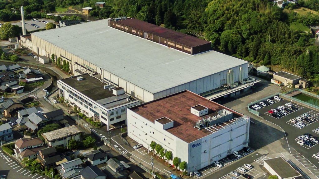 ATJ5 – 大分
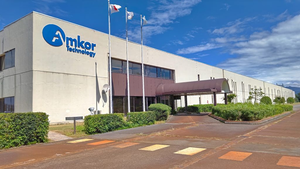 ATJ6 – 福井
 ATJ7 – 函館
Amkor Technology Malaysia(ATM)は、マレーシアのフリーインダストリアルゾーン内に位置し、クアラルンプール市中心部およびクアラルンプール国際空港から約50kmの距離にあります。自由貿易地域の便利な物流とビジネスに有利な政策により、Amkorの顧客は付加価値税や免税を通じて世界中に商品を配送することができます。ATMには32,000平方メートルの製造スペースと108,800平方メートルの土地を有します。
提供サービス
- パッケージテスト
Packages
- SO8-FL
- SONXXX-FL
- TO-220FP
- TQFP
- TSON-FL
マーケット
- ディスクリート
- Power
 エンドオブライン(EOL)
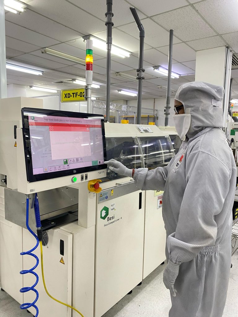 SO8パッケージファイナルテスト
 ATM1 – マレーシア
Amkor Technology Philippines(ATP)は、アセンブリおよびテストに関するフルレンジのサービスを提供しています。ATPは、ムンティンルパ市(P1)およびラグナ州ビニャン市(P3/P4)に2つの工場を構え、世界中のお客様のニーズに対応しています。ムンティンルパ市のATP P1工場は、32,000平方メートルの製造スペースを有し、レガシーリードフレーム製品の生産に特化しています。
ATP P3/P4は、フィリピン・ラグナ州ビニャン市に位置し、32,800平方メートルの敷地を有し、先進パッケージング技術の分野をリードしています。P3のアセンブリ拠点は、先端パッケージで高く評価されており、MEMSおよびセンサーの製造・開発拠点として機能しています。P4にあるAmkorのテスト施設では、過去30年間にわたり、パワー、マイコン、MEMSなど幅広い用途に対応したウェーハプローブおよび最終テストサービスを提供してきました。
ATPはフィリピン経済区庁(PEZA)に登録されており、Amkorの顧客はさまざまなメリットを享受できます。これらのメリットには、インセンティブ付きでの製品の世界各地への出荷、VAT(付加価値税)のゼロ税率、優遇税率などが含まれており、コスト効率に優れた、効率的なサプライチェーンの実現を可能にします。
ATPは、信頼性の高いパッケージング技術の革新とテスト設備において高い評価を得ています。生産機能と製品開発を兼ね備えた運営体制により、半導体業界の変化するニーズに柔軟に対応しています。
提供サービス
- ウェハプローブ
- パッケージテスト
- フィルムフレームテスト
- システムレベルテスト
- テスト開発
- MEMSテスト
- バーンイン
Packages
- MLF®
- リードフレーム
- QFP
マーケット
- 自動車向け
- 民生品
- メモリ
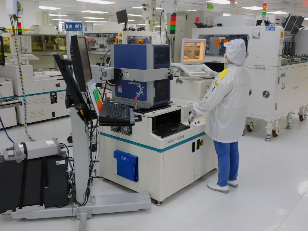 ウェハプローブ
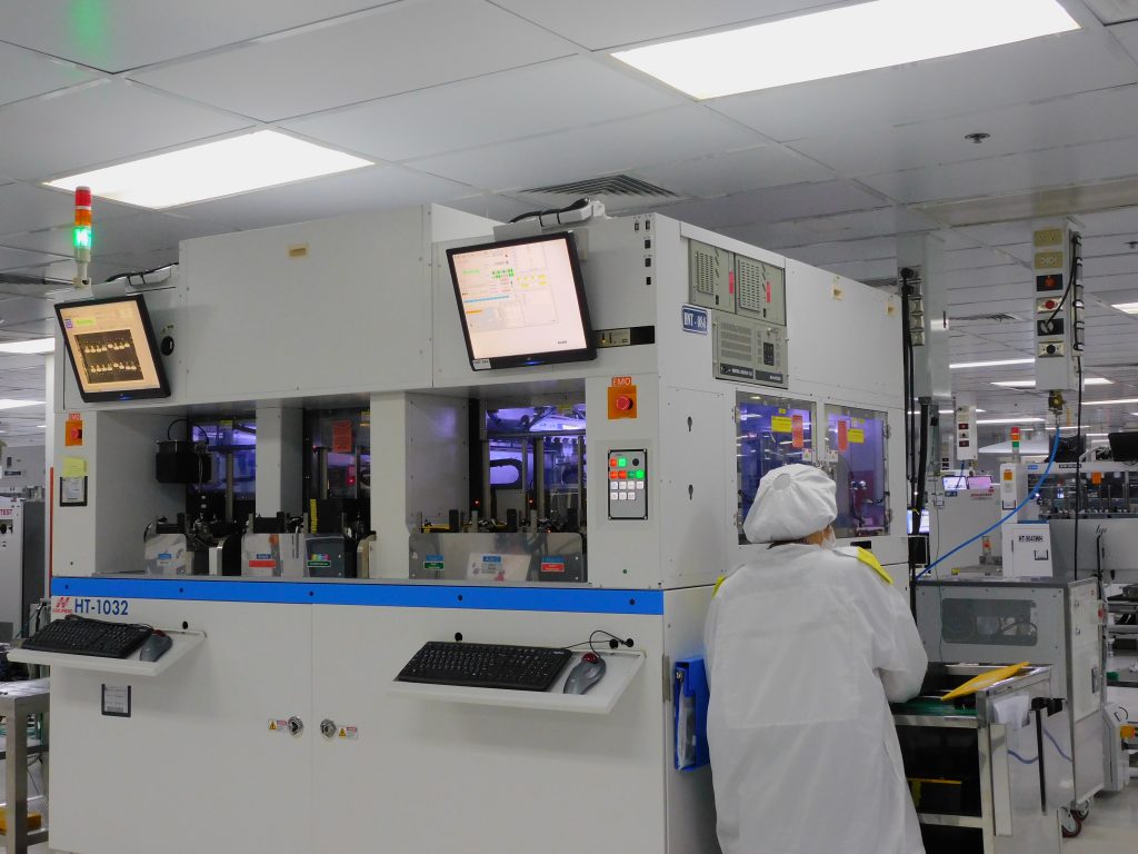 最終テスト:ピック&プレイスハンドラ
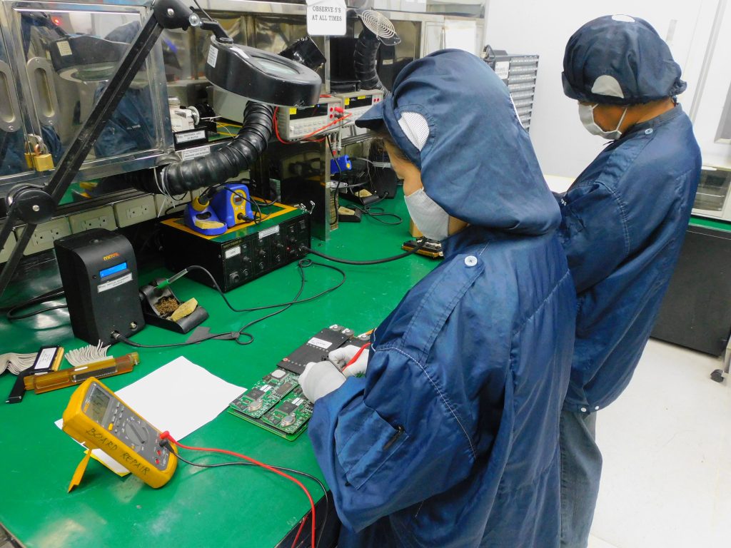 テストハードウェア修理ステー
ション
 最終試験重力フィードハンドラ
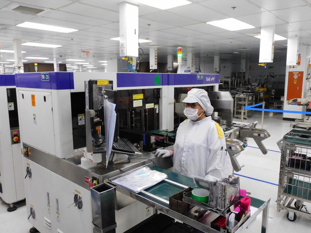 ポストテストテープ&リールハンドラ
 バーンイン手動ロードおよびアンロード
 ATP3/P4 – フィリピン
Amkor Technology Vietnam(ATV)はバクニンに位置しており、空港までの所要時間は25分です。この拠点では、システム・イン・パッケージおよびメモリパッケージの製造・テストサービスを提供しています。さらにATVは、パッケージ設計、テストプログラム、組立て開発を含む包括的なソリューション設計を支援するための研究開発リソースも提供しています。また、ATVは広大なクリーンルーム製造スペースを有しています。
提供サービス
- バーンインテスト
- パッケージテスト
- システムレベルテスト
- テスト開発
- ウェハプローブ
Packages
- DPS
- SiP – DSMBGA
- SiP – DSLGA
- Stacked CSP
マーケット
- コミュニケーション
- 民生品
- メモリ
 SLT
SLT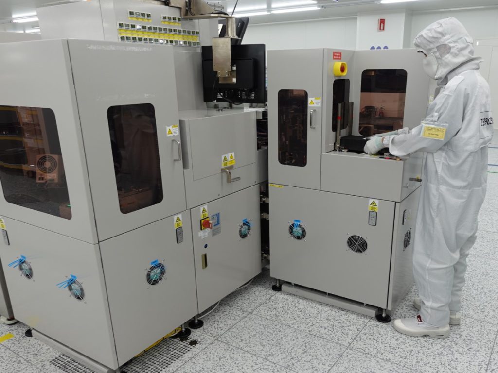 スキャン
スキャン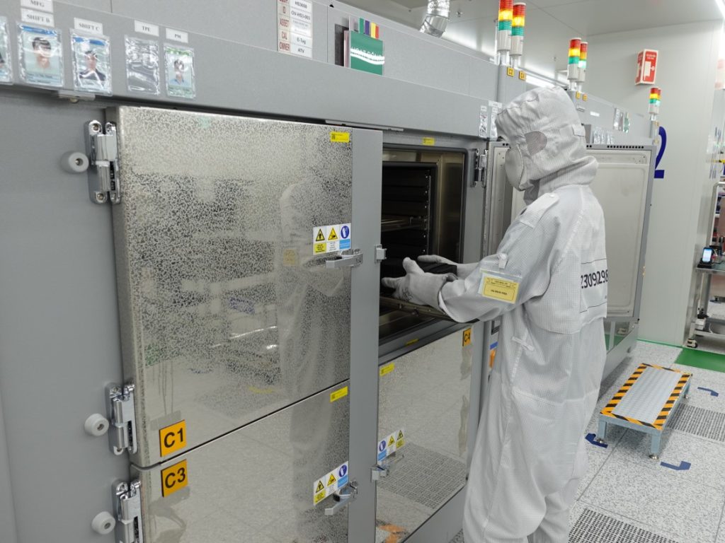 ベーク
ベーク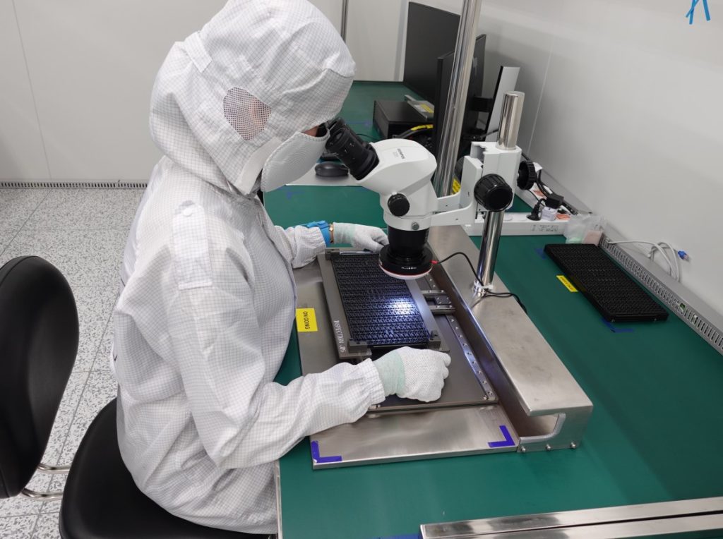 最終外観検査チェック
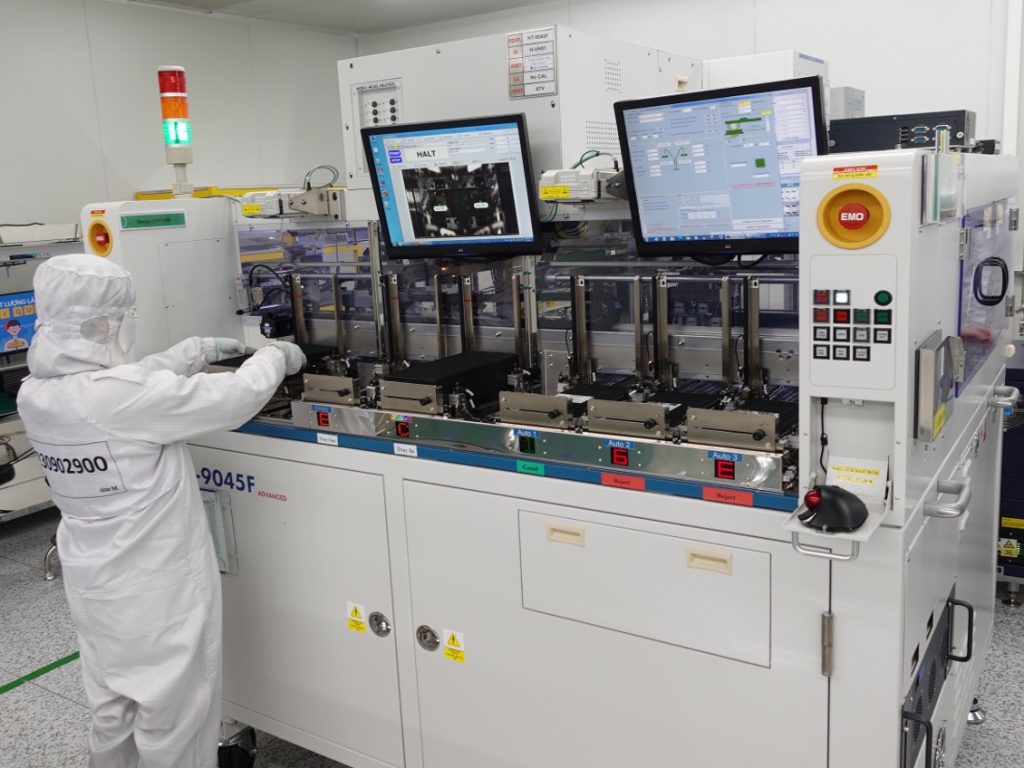 ピック&プレイスハンドラによる最終テスト
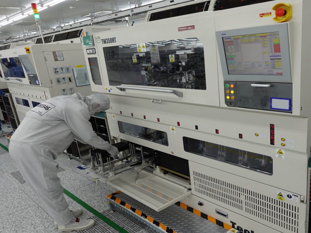 メモリテストハンドラ
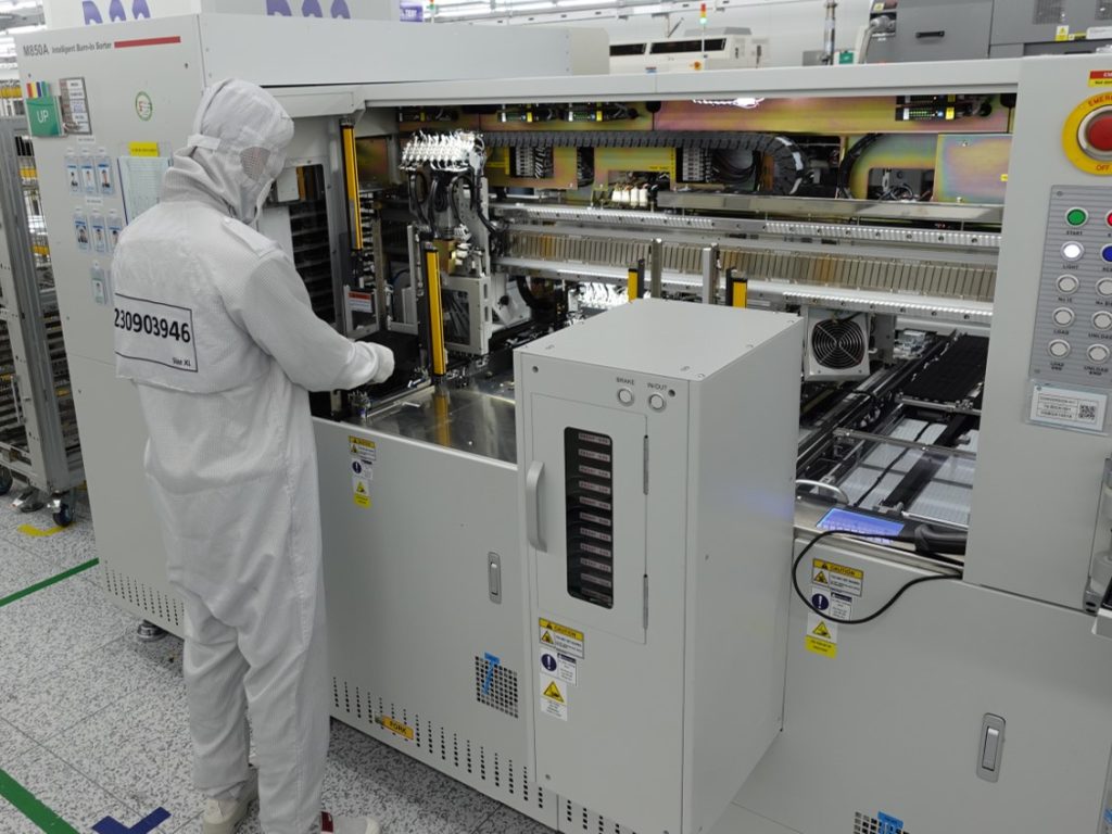 メモリテストセル
 テストハードウェア修理ステー
ション
 ATV – ベトナム
Amkor Technology Portugal(ATEP)は、ポルトガル第2の都市であるポルト近郊に位置しており、国際空港および港湾からわずか15分という距離にあり、ヨーロッパ各地および世界各国への優れた直通アクセスを有しています。ATEPは、先端パッケージングに特化したヨーロッパ最大の半導体後工程受託製造(OSAT)拠点であり、この地域では50年以上にわたり半導体の組立・テストの経験が蓄積されています。現在、ATEPは20,000平方メートルのクリーンルームスペースを有しており、これを50,000平方メートルまで拡張中です。
提供サービス
- ウェハプローブ
- テスト開発
Packages
- FCBGA
- WLCSP
- WLFO
マーケット
- 自動車向け
- コミュニケーション
- メモリ
 オープン&ショートテストハンドラ
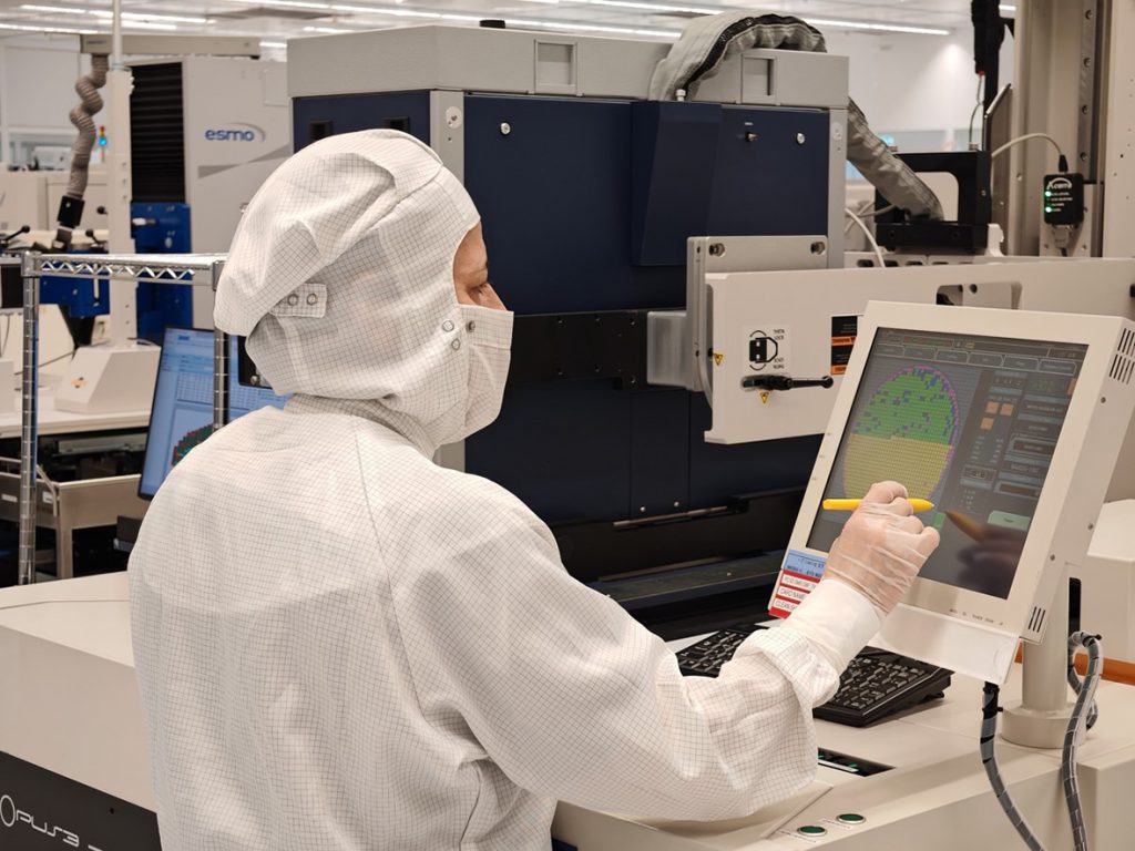 Cohuテスター
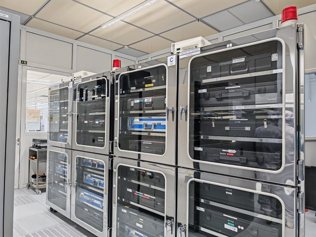 テストハードウェアストレージシステム
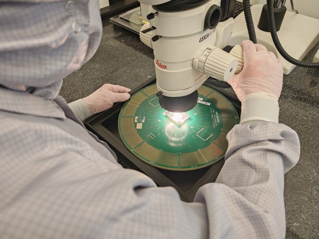 テストハードウェア修理ステー
ション
 V93000ウェハープローブテストセル
 Cohu/Semicsウェハープローブテストセル
 Ultraflexウェハープローブテストセル
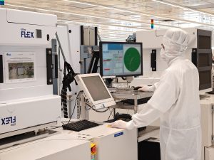 Ultraflexウェハープローブテストセル
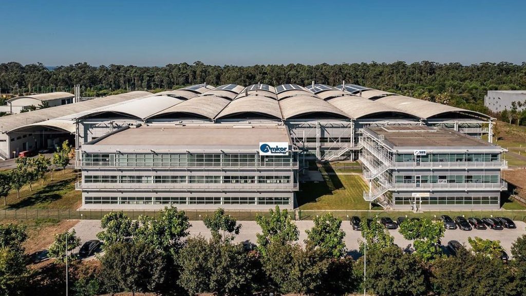 ATEP – ポルトガル
Amkor Technology China(ATC)は、中国(上海)の自由貿易試験区に位置しており、上海の主要な2つの空港から約30キロメートルの距離にあります。自由貿易地域の便利な物流とビジネスに有利な政策により、Amkorの顧客は付加価値税や免税を通じて世界中に商品を配送することができます。ATCは17万平方メートルの製造スペースを有しています。
提供サービス
- ウェハプローブ
- フィルムフレームテスト
- パッケージテスト
- バーンインテスト
- システムレベルテスト
- テスト開発
Packages
- CSP
- FCBGA
- フリップチップ
- MLF®/QFN
- PBGA
- WLCSP
マーケット
- 自動車向け
- コミュニケーション
- 民生品
- 産業向け
 バーンイン
バーンイン ファイナルテスト
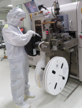 エンドオブライン(EOL)
 メモリテストセル
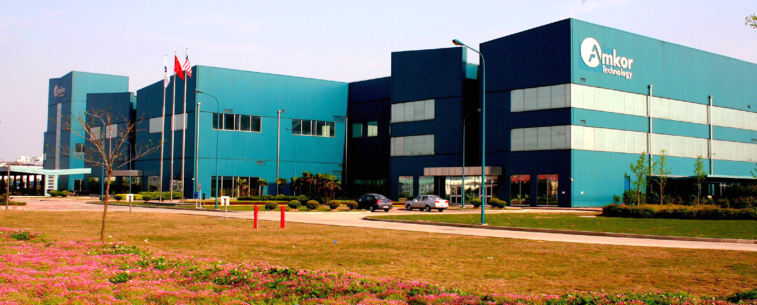 ATC1 – 上海
テスト開発エンジニアリング
お客様は自社でテストソリューションを開発し、量産時にAmkorへ委託することが可能です。Amkorとのソフトウェアやハードウェアの共同開発、またすべての開発をAmkorへご依頼頂くことも可能です。最大限のパフォーマンスを発揮するためには製品設計の早期のタイミングから当社と連携頂くことがベストですが、製品ライフサイクルの後半でコスト効率の高いテスターおよび(または)高度な多数個同時測定への移行を行うことでも大幅なコストダウンを提供いたします。
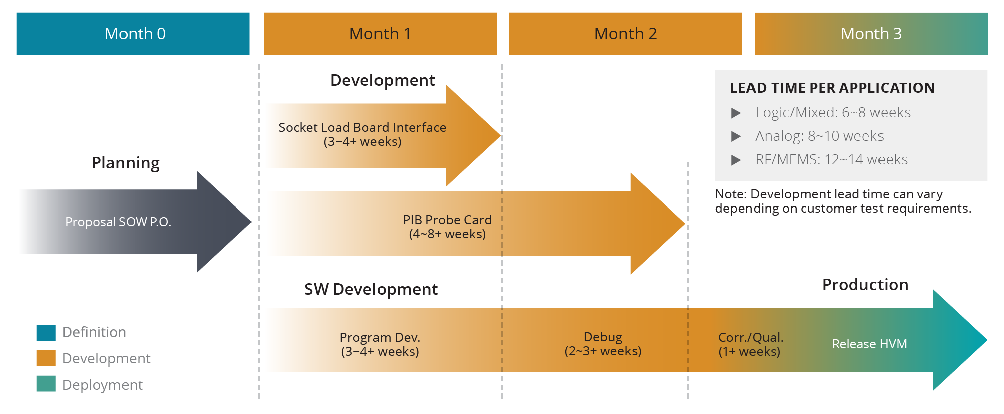
一般的なテスト開発のサイクルタイム

市場別差別化テスト
Amkorは自動車向けOSATとしてNo.1サプライヤーであり、ワールドワイドレベルでサプライチェーンをサポートします。この領域の製品には、ハイレベルの性能が要求される安全性に関する製品やインフォテインメント(ADAS)に関する物が含まれています。これには、本番テストワークフロー中に包括的なテストセットが必要です。
- コールドウェーハプローブ、常温および高温での最終テスト
- 高品質で規格に準拠したプロセスおよびシステム
- 検査および複数温度テストに対応
- ウェハプローブ:-55°C~+200°C
- -55°C ~ +175°Cでのファイナルテスト
- バーンイン
- システムレベルテスト(SLT)
- 低温ウェハプローブを活用することで、ファイナルテストは室温と高温のみのテストを行います
- 組立後のオープン/ショートテストには、2線および4線式の抵抗測定が含まれます
Amkorの収益の大部分は、通信市場セグメントから得られています。このセグメントには、スマートフォン、タブレット、携帯型端末、ウェアラブルデバイスが含まれます。当社の最先端のテストソリューションは携帯電話やコネクティビティ技術などに求められる要件の急速な変化に柔軟に対応します。Amkorは、5Gおよび6GのRFワイヤレス製品とそのテスト要件に対して、万全の対応体制を整えています。
- FR1とFR2の両方の周波数範囲に対するRF 5G NR導電性テスト
- さまざまなRF接続性規格のための非同期テスト
- 32ポート、マルチサイト、マルチチャネル Tx/Rx対応ATE
- RF コールボックステスト含むシンプルなSLTを使用し複雑なSiPに対応
- ローカルRFシールディング ≤60 dBm
- コストを低減するマルチサイトx8 RFテスト
- RFフロントエンド(RFFE)、SiPおよび IoT
- WLCSP向けKnown Goood Die(KGD)、SiP向けKnown Tested Die(KTD)のRFウェハプローブ対応
- 単一および複数チャネルのビームフォーミング、位相配列、AiP/AoP対応
- SoC + メモリ PoPーダブルサイドテスト/スタック CSP - メモリおよびロジックテスト
Amkorは、ネットワーキングおよびハイパフォーマンスコンピューティング市場における高性能テストソリューションのリーディングプロバイダーです。この市場セグメントでは、AIアクセラレータ、CPU、GPU、FPGA、I/O、SERDES(PCIe、CXL)、シリコンフォトニクスなどを含む複数のチップレットに対する需要が高まっています。これらの市場において不可欠なのが、高帯域幅メモリ(HBM)などの先進的なメモリ技術や、HDDからNANDベースのSSDへの移行です。
- 2.5Dおよび3D実装においては、ウェーハプローブ、主要なアセンブリ工程間でのインシチュテスト、最終テスト(SLTおよびATE)を含む分散型テストに対応しています。また、Chip-on-Wafer(CoW)向けのプローブソリューションおよびウェーハマップ管理も提供しています
- SLTおよびATEテストにおいて、最大300ワットと最大1000ワットの製品に対応した、低温・常温・高温の3温度領域でのアクティブサーマルコントロール(ATC)を提供
- 動的バーンインおよびバーンイン中テスト(TDBI)
- フィルムフレームおよびストリップテスト(x308 EEPROM)
- 最大 16 Gbps および 32 Gbpsまでの高速シリアルデジタルの検査(例:PCIe、第4世代、第5世代)
- シリコンフォトニクスIC
Amkorは、自動車、送電、産業分野向けのダイオード、フリップチップMOSFET、インテリジェントパワーモジュール、絶縁ゲートバイポーラトランジスタ(IGBT)、マルチ電圧FET、レギュレータ、バイポーラトランジスタなどのパワーディスクリートデバイスおよびモジュールにおけるリーダーです。Amkorのテストサービスは、サイクルタイムの短縮とコスト削減を実現するために、組立フローと緊密に統合されています。以下が主な特徴です:
- 高電流、高電圧
- ケルビンコンタクトタイプテスト
- 低 Rds_on
- Si、SiC、Gan
今日のモノのインターネット(IoT)と産業用IoT(IIoT)製品にはMCU、RF送/受信機、センサー、アクチュエータが必要になります。センサー技術には、磁力計、加速度計、ジャイロスコープ、近接、RFスイッチ、フォトセンサー、マイク、マイクロスピーカー、湿度、圧力、温度が含まれますが、これらに限定されません。テストソリューションは、さまざまな業務範囲におけるこれらの物理的で実世界のアナログ信号を、製造ワークフロー中にテストされた電気刺激に変換する必要があります。
ご質問やお問合せはこちらまで
以下の「リクエスト」をクリックしてご連絡ください